ARCHIVE 2009 - BiTS Workshop
ARCHIVE 2009 - BiTS Workshop
ARCHIVE 2009 - BiTS Workshop

You also want an ePaper? Increase the reach of your titles
YUMPU automatically turns print PDFs into web optimized ePapers that Google loves.
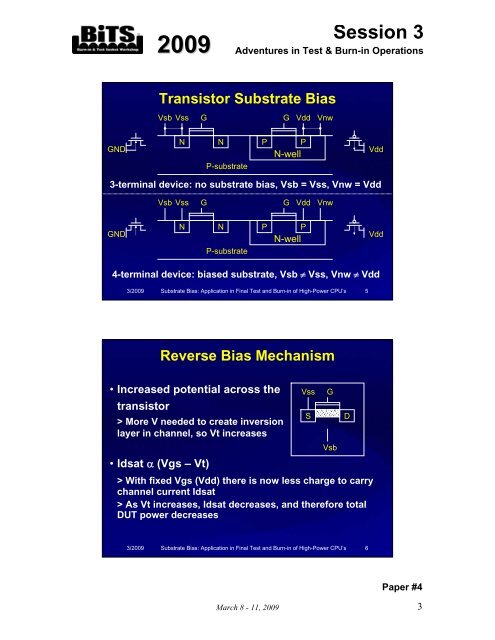
<strong>2009</strong>Session 3Adventures in Test & Burn-in OperationsTransistor Substrate BiasVsb Vss GG Vdd VnwGNDNNP-substratePPN-wellVdd3-terminal device: no substrate bias, Vsb = Vss, Vnw = VddVsbVssGGVddVnwGNDNNP-substratePPN-wellVdd4-terminal device: biased substrate, Vsb ≠ Vss, Vnw ≠ Vdd3/<strong>2009</strong> Substrate Bias: Application in Final Test and Burn-in of High-Power CPU’s 5Reverse Bias Mechanism• Increased potential across thetransistor> More V needed to create inversionlayer in channel, so Vt increases• Idsat α (Vgs – Vt)Vss> With fixed Vgs (Vdd) there is now less charge to carrychannel current Idsat> As Vt increases, Idsat decreases, and therefore totalDUT power decreasesSGVsbD3/<strong>2009</strong> Substrate Bias: Application in Final Test and Burn-in of High-Power CPU’s 6Paper #4March 8 - 11, <strong>2009</strong>3