Jens Janssen Diploma Thesis - Prof. Dr. Norbert Wermes ...
Jens Janssen Diploma Thesis - Prof. Dr. Norbert Wermes ...
Jens Janssen Diploma Thesis - Prof. Dr. Norbert Wermes ...

You also want an ePaper? Increase the reach of your titles
YUMPU automatically turns print PDFs into web optimized ePapers that Google loves.
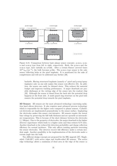
p-on-n typen-on-n typeguard rings p + -type pixel implantsn + -type pixel implantsbefore type inversionn-on-p typen + -type pixel implantsguard ringsdepletedn-substratedepleteddepletedp-substraten + -type backside guard rings p + -type backside p + -type backsideafter type inversiondepleted“p”-substratedepleted(no type inversion)Figure 3.15: Comparison between basic planar sensor concepts: p-on-n, n-onnand n-on-p type from left to right, respectively. Both, the p-on-n and then-on-n type, have initially an n-bulk. After a certain fluence (several times10 12 n eq /cm ≠2 ), the bulk becomes p-like. The p-on-n type sensor is the onlysensor collecting holes at the pixel implants. It is mentioned for the sake ofcompleteness and will not be addressed any further [29].backside. Having structured implants (namely n + -pixel and p-stop/sprayimplants) only on one side makes this sensor cost-e ective [31]. In addition,the sensor can easily be thinned down. This reduces the materialbudget and improves tracking performance. A major drawback are possibledischarges at the cutting edge of the sensor into the readout chip[32]. Although the sensor is biased from the back side the potential drophappens at the front side. A multi guard ring structure on the pixel sideensures the potential drop towards the pixel implants.3D Sensors 3D sensors are the most advanced technology concerning radiationhard silicon detectors. It also requires most advanced process technologywhich is responsible for the higher costs compared to planar sensors. Cylindricalelectrodes are implemented perpendicular to the sensor surface. Implantingthe electrodes makes this sensor cost-intensive. 3D sensors require the lowestbias voltage by preserving the full bulk thickness and are operable at intermediatetemperatures. This is because of the short distance between the electrodes(Æ 100 µm). Due to the geometry of electrodes, the major drawback is the higherdetector capacitance which leads to a higher noise and thus reduces S/N ratio.Another drawback is the reduced hit detection probability and charge collectione ciency for normal incidence. This only a ects ionizing particles traversingthe sensor electrodes. The detector recover full e ciency under a certain incidentangle. Another possibility is the implementation of the electrodes under acertain angle into the bulk.Two di erent design concepts are proposed for the IBL upgrade [27]: Singlesided(“full-3D”) with active edges and double-sided 3D sensors. The activeedge technology allows a minimum of dead area at the edge of the sensor (a31