Jens Janssen Diploma Thesis - Prof. Dr. Norbert Wermes ...
Jens Janssen Diploma Thesis - Prof. Dr. Norbert Wermes ...
Jens Janssen Diploma Thesis - Prof. Dr. Norbert Wermes ...

Create successful ePaper yourself
Turn your PDF publications into a flip-book with our unique Google optimized e-Paper software.
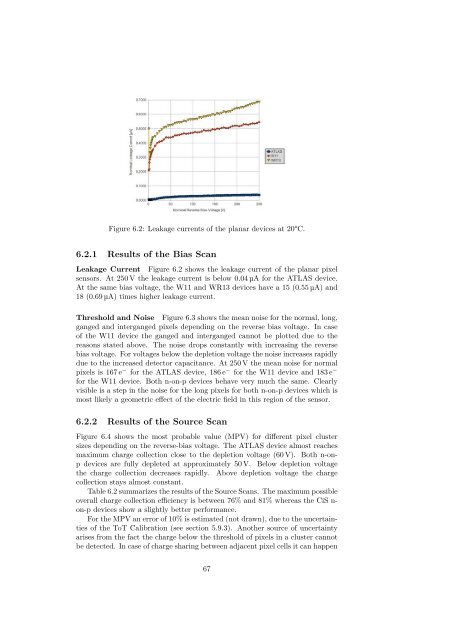
Figure 6.2: Leakage currents of the planar devices at 20°C.6.2.1 Results of the Bias ScanLeakage Current Figure 6.2 shows the leakage current of the planar pixelsensors. At 250 V the leakage current is below 0.04 µA for the ATLAS device.At the same bias voltage, the W11 and WR13 devices have a 15 (0.55 µA) and18 (0.69 µA) times higher leakage current.Threshold and Noise Figure 6.3 shows the mean noise for the normal, long,ganged and interganged pixels depending on the reverse bias voltage. In caseof the W11 device the ganged and interganged cannot be plotted due to thereasons stated above. The noise drops constantly with increasing the reversebias voltage. For voltages below the depletion voltage the noise increases rapidlydue to the increased detector capacitance. At 250 V the mean noise for normalpixels is 167 e ≠ for the ATLAS device, 186 e ≠ for the W11 device and 183 e ≠for the W11 device. Both n-on-p devices behave very much the same. Clearlyvisible is a step in the noise for the long pixels for both n-on-p devices which ismost likely a geometric e ect of the electric field in this region of the sensor.6.2.2 Results of the Source ScanFigure 6.4 shows the most probable value (MPV) for di erent pixel clustersizes depending on the reverse-bias voltage. The ATLAS device almost reachesmaximum charge collection close to the depletion voltage (60 V). Both n-onpdevices are fully depleted at approximately 50 V. Below depletion voltagethe charge collection decreases rapidly. Above depletion voltage the chargecollection stays almost constant.Table 6.2 summarizes the results of the Source Scans. The maximum possibleoverall charge collection e ciency is between 76% and 81% whereas the CiS n-on-p devices show a slightly better performance.For the MPV an error of 10% is estimated (not drawn), due to the uncertaintiesof the ToT Calibration (see section 5.9.3). Another source of uncertaintyarises from the fact the charge below the threshold of pixels in a cluster cannotbe detected. In case of charge sharing between adjacent pixel cells it can happen67