Jens Janssen Diploma Thesis - Prof. Dr. Norbert Wermes ...
Jens Janssen Diploma Thesis - Prof. Dr. Norbert Wermes ...
Jens Janssen Diploma Thesis - Prof. Dr. Norbert Wermes ...

Create successful ePaper yourself
Turn your PDF publications into a flip-book with our unique Google optimized e-Paper software.
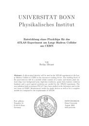
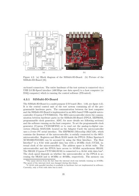
(a)Figure 4.2: (a) Block diagram of the S3Multi-IO-Board.S3Multi-IO-Board [35].(b)(b) Picture of theon-board connectors. The entire hardware of the test system is connected via aUSB 2.0 Hi-Speed interface (480 Mbps raw data speed) to a host computer (orDAQ computer) which is running the control software (STcontrol).4.3.1 S3Multi-IO-BoardThe S3Multi-IO-Board is a multi-purpose I/O board (Rev. 1.03, see figure 4.2).It is the central control unit of the test system containing all of the programmablehardware parts. The communication between the host computerand the S3Multi-IO-Board is implemented in an 8051-based USB-capable microcontroller(Cypress CY7C68013A). The 8051-microcontroller steers the communicationbetween hardware parts on the S3Multi-IO-Board (FPGA, EEPROM,programmable clock generator, ADC; for more details see following sections)and the software running on the host computer. To set the programmable clockgenerator (Cypress CY22150FZXI) or to read out the analog-to-digital converters(Maxim MAX1238, located on the Adapter Card) the microcontrolleruses a 2-wire I C serial interface. The EEPROM (Microchip 24LC128), whichcontains the firmware of the microcontroller, is serially connected to the 8051-microcontroller. Registers and Block RAM inside the FPGA (Xilinx Spartan-3XC3S1000-FGG320) can be accessed by using the Slow Interface. The SlowInterface 3 is a 8-bit wide parallel data bus with a 48 MHz clock (UCLK, internalclock of the microcontroller). The address space is 16-bit wide. Themicrocontroller and the FPGA have access to 16 Mbit asynchronous SRAM.The SRAM (Cypress CY7C1061AV33) is connected to a 16-bit wide data bus 4 .The clock speed depends on whether the microcontroller or the FPGA is accessingthe SRAM and is 48 MHz or 40 MHz, respectively. The memory can3 The name derives from the fact that the internal clock was initially running on 24 MHz.The speed of the internal clock was changed during this thesis.4 A16-bitwideparallelinterfaceisavailableinhardwarebutnotimplementedinsoftware.Currently, only a 8-bit wide data bus is used.35