Jens Janssen Diploma Thesis - Prof. Dr. Norbert Wermes ...
Jens Janssen Diploma Thesis - Prof. Dr. Norbert Wermes ...
Jens Janssen Diploma Thesis - Prof. Dr. Norbert Wermes ...

You also want an ePaper? Increase the reach of your titles
YUMPU automatically turns print PDFs into web optimized ePapers that Google loves.
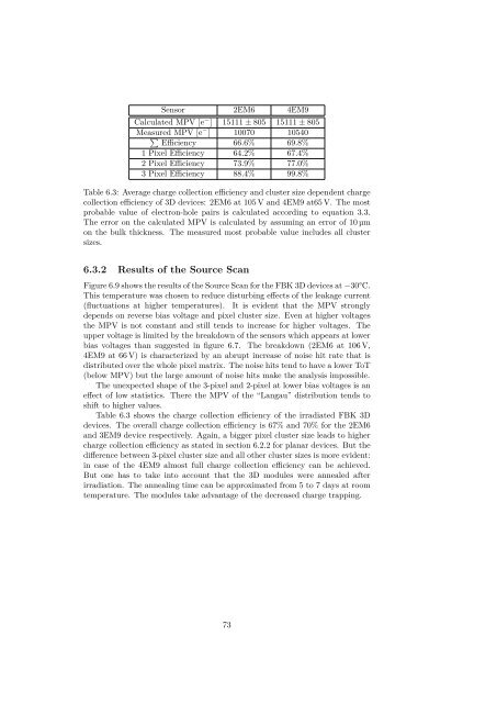
Sensor 2EM6 4EM9Calculated MPV [e ≠ ] 15111 ± 805 15111 ± 805MeasuredqMPV [e ≠ ] 10070 10540E ciency 66.6% 69.8%1PixelE ciency 64.2% 67.4%2PixelE ciency 73.9% 77.0%3PixelE ciency 88.4% 99.8%Table 6.3: Average charge collection e ciency and cluster size dependent chargecollection e ciency of 3D devices: 2EM6 at 105 V and 4EM9 at65 V. The mostprobable value of electron-hole pairs is calculated according to equation 3.3.The error on the calculated MPV is calculated by assuming an error of 10 µmon the bulk thickness. The measured most probable value includes all clustersizes.6.3.2 Results of the Source ScanFigure 6.9 shows the results of the Source Scan for the FBK 3D devices at ≠30°C.This temperature was chosen to reduce disturbing e ects of the leakage current(fluctuations at higher temperatures). It is evident that the MPV stronglydepends on reverse bias voltage and pixel cluster size. Even at higher voltagesthe MPV is not constant and still tends to increase for higher voltages. Theupper voltage is limited by the breakdown of the sensors which appears at lowerbias voltages than suggested in figure 6.7. The breakdown (2EM6 at 106 V,4EM9 at 66 V) is characterized by an abrupt increase of noise hit rate that isdistributed over the whole pixel matrix. The noise hits tend to have a lower ToT(below MPV) but the large amount of noise hits make the analysis impossible.The unexpected shape of the 3-pixel and 2-pixel at lower bias voltages is ane ect of low statistics. There the MPV of the “Langau” distribution tends toshift to higher values.Table 6.3 shows the charge collection e ciency of the irradiated FBK 3Ddevices. The overall charge collection e ciency is 67% and 70% for the 2EM6and 3EM9 device respectively. Again, a bigger pixel cluster size leads to highercharge collection e ciency as stated in section 6.2.2 for planar devices. But thedi erence between 3-pixel cluster size and all other cluster sizes is more evident:in case of the 4EM9 almost full charge collection e ciency can be achieved.But one has to take into account that the 3D modules were annealed afterirradiation. The annealing time can be approximated from 5 to 7 days at roomtemperature. The modules take advantage of the decreased charge trapping.73