- Page 2 and 3:
This text was adapted by The Saylor
- Page 4 and 5:
third, it provides a review for tho
- Page 6 and 7:
Chapter 1 Introduction to Chemistry
- Page 8 and 9:
accounting for only 0.0000001% of E
- Page 10 and 11:
eginning scientist who intends to s
- Page 12 and 13:
elements by mass. Thus sodium chlor
- Page 14 and 15:
Strategy: Refer to the definitions
- Page 16 and 17:
Chemists study the structures, phys
- Page 18 and 19:
kerosene, diesel fuel, and lubricat
- Page 20 and 21:
Solution: a. A Tea is a solution of
- Page 22 and 23:
centimeter (g/cm 3 ). As mass incre
- Page 24 and 25:
contrast, the mass of sample E is s
- Page 26 and 27:
e. the sensitivity of the volume to
- Page 28 and 29:
15. Classify each statement as an e
- Page 30 and 31:
8. Gold has a density of 19.30 g/cm
- Page 32 and 33:
know to be carbon dioxide, is the s
- Page 34 and 35:
as did the first. But what was the
- Page 36 and 37:
. Ratios of 3.0 and 2.0 give 1.8 g
- Page 38 and 39:
Summary The ancient Greeks first pr
- Page 40 and 41:
1. Electrons and protons have elect
- Page 42 and 43:
well before he was run over by a ho
- Page 44 and 45:
In a single famous experiment, howe
- Page 46 and 47:
The dates in parentheses are the ye
- Page 48 and 49:
C O N C E PTUAL P R OBLEMS 1. Descr
- Page 50 and 51:
As described in Section 1.7 "Introd
- Page 52 and 53:
In with 8 neutrons and 6 protons. T
- Page 54 and 55:
Solution: A The element with 82 pro
- Page 56 and 57:
the isotopes. Because most elements
- Page 58 and 59:
The mass of an atom is a weighted a
- Page 60 and 61:
2. Determine the number of protons,
- Page 62 and 63:
The elements are arranged in a peri
- Page 64 and 65:
exhibit manic-depressive, or bipola
- Page 66 and 67:
f. nickel g. potassium h. radon i.
- Page 68 and 69:
10. Based on their locations in the
- Page 70 and 71:
emoved, minimize inadvertent contam
- Page 72 and 73:
supplements. Second, as shown in Fi
- Page 74 and 75:
Measurement Instruments of Measurem
- Page 76 and 77:
Base Quantity Unit Name Abbreviatio
- Page 78 and 79:
g. 2002.080 h. 0.01020 Solution a.
- Page 80 and 81:
( 6 .0 22 × 1 0 23 ) ( 6 . 42 × 1
- Page 82 and 83:
f. infinite (rule 5) S K I L L BUIL
- Page 84 and 85:
In the worked examples in this text
- Page 86 and 87:
The deviations are 1.125 g − 1.11
- Page 88 and 89:
Please be sure you are familiar wit
- Page 90 and 91:
Isotope Percent Abundance (%) Atomi
- Page 92 and 93:
2.1 Chemical Compounds L E A R N I
- Page 94 and 95:
Compounds that consist primarily of
- Page 96 and 97:
a. Nitrous oxide, also called “la
- Page 98 and 99:
Figure 2.3 The Three-Dimensional St
- Page 100 and 101:
group or as a water molecule in whi
- Page 102 and 103:
Answer: a. CHCl 3 a. N 2H 4 b. C 4H
- Page 104 and 105:
Figure 2.6 The Effect of Charge and
- Page 106 and 107:
Predict the charge on the most comm
- Page 108 and 109:
(a) The positively and negatively c
- Page 110 and 111:
1. The structural formula for chlor
- Page 112 and 113:
ANSWERS 5. a. 27 b. 38 c. 54 d. 28
- Page 114 and 115:
Asked for: empirical formula for bi
- Page 116 and 117:
Formula NH4 + CH3NH3 + OH − O2 2
- Page 118 and 119:
. A The potassium cation is K + , a
- Page 120 and 121:
d. H 2 S e. NaC 2 H 3 O 2 4. Genera
- Page 122 and 123:
. B 2 H 6 c. C 6 H 12 O 6 d. P 4 O
- Page 124 and 125:
1. Place the ions in their proper o
- Page 126 and 127:
more oxygen atoms ends in -ate, and
- Page 128 and 129:
Write the systematic name (and the
- Page 130 and 131:
Compounds and Covalent Molecular Su
- Page 132 and 133:
2− h. C 2 O 4 3. Name each anion.
- Page 134 and 135:
A N S W E R 1. a. rubidium bromide
- Page 136 and 137:
a. sodium hydroxide b. calcium cyan
- Page 138 and 139:
. Prefixes derived from Greek stems
- Page 140 and 141:
a. A Because sulfur is to the left
- Page 142 and 143:
in Chapter 7 "The Periodic Table an
- Page 144 and 145:
Name Number of Carbon Atoms Molecul
- Page 146 and 147:
groups are on the same side of the
- Page 148 and 149:
alkane, the alkene, or the alkyne.
- Page 150 and 151:
c. 2-butyne d. cyclooctene Given: n
- Page 152 and 153:
c. HC≡C(CH 2) 4CH 3 d. e. The gen
- Page 154 and 155:
ends of the chain connected to form
- Page 156 and 157:
e. 7. For each structural formula,
- Page 158 and 159:
. neptunium(IV) oxide c. iron(II) s
- Page 160 and 161:
e. 2.5 Acids and Bases LEARNING OBJ
- Page 162 and 163:
Figure 2.20 The Relationship betwee
- Page 164 and 165:
Figure 2.21 Some Common Carboxylic
- Page 166 and 167:
Common acids and the polyatomic ani
- Page 168 and 169:
f. H 2 SO 4 7. Draw the structure o
- Page 170 and 171:
4. Name each compound. a. H 2 SO 4
- Page 172 and 173:
chemicals are either fertilizers (a
- Page 174 and 175:
accomplish this transformation is c
- Page 176 and 177:
years was tetraethyllead [(C2H5)4Pb
- Page 178 and 179:
(from the Latin vitrum, meaning “
- Page 180 and 181:
(K2O). The usual source of potassiu
- Page 182 and 183:
7. ♦ Sodamide, or sodium amide, i
- Page 184 and 185:
As you learned in Chapter 1 "Introd
- Page 186 and 187:
E X A M P L E 2 Calculate the formu
- Page 188 and 189:
12—is also arbitrary. The importa
- Page 190 and 191:
chemists to calculate the mass of a
- Page 192 and 193:
mass of ethylene glycol (g) molar m
- Page 194 and 195:
a. 1.71 g b. 0.721 g Summary The mo
- Page 196 and 197:
. c. d. e. 5. Calculate the molar m
- Page 198 and 199:
a. b. 8. Calculate the number of mo
- Page 200 and 201:
Substance Mass (g) Number of Moles
- Page 202 and 203:
We could also calculate the mass pe
- Page 204 and 205:
Determining the Empirical Formula o
- Page 206 and 207:
possible. To obtain whole numbers,
- Page 208 and 209:
Because there are two phosphorus at
- Page 210 and 211:
A Use the masses and molar masses o
- Page 212 and 213:
lood. At this point, we cannot know
- Page 214 and 215:
C Multiply each subscript in the em
- Page 216 and 217:
The empirical formula of a substanc
- Page 218 and 219:
15. Calculate the mass percentage o
- Page 220 and 221:
2. Salicylic acid is used to make a
- Page 222 and 223:
23. a. 27.6 mg C and 1.98 mg H b. 5
- Page 224 and 225:
sides. Equation 3.9 and Equation 3.
- Page 226 and 227:
Construct a table showing how to in
- Page 228 and 229:
Equation 3.11 C 7 H 16 (l) + O 2 (g
- Page 230 and 231:
Given: reactants and product Asked
- Page 232 and 233:
4. What information can be obtained
- Page 234 and 235:
A balanced chemical equation gives
- Page 236 and 237:
mass of CO 2 = 1 .51 mol CO 2 × 44
- Page 238 and 239:
The volatility and toxicity of merc
- Page 240 and 241:
4. Convert the number of moles of p
- Page 242 and 243:
B We need to calculate the number o
- Page 244 and 245:
Given: masses of reactants and prod
- Page 246 and 247:
The stoichiometry of a reaction des
- Page 248 and 249:
e. 10.648 g of Ba 3 (PO 4 ) 2 f. 5.
- Page 250 and 251:
13. Under the proper conditions, am
- Page 252 and 253:
2 PaI 5 (s) → Δ 2 Pa(s) + 5I 2 (
- Page 254 and 255:
c. 0.923 kg K 3 PO 4 d. 0.458 kg Ni
- Page 256 and 257:
Familiarity with a few basic types
- Page 258 and 259:
equal the total of electrons gained
- Page 260 and 261:
oxidation state of oxygen is determ
- Page 262 and 263:
. Note that (NH 4) 2SO 4 is an ioni
- Page 264 and 265:
oxidant + reductant → oxidation
- Page 266 and 267:
The following reactions have import
- Page 268 and 269:
Using Table 3.1 "Basic Types of Che
- Page 270 and 271:
eduction reaction, one atom must lo
- Page 272 and 273:
N U M E R I C A L PR O BL E M S Ple
- Page 274 and 275:
8. For each redox reaction, determi
- Page 276 and 277:
15. The reaction of X 4 (orange) wi
- Page 278 and 279:
. Na, +1; Cl, −1 c. O, −2; C, +
- Page 280 and 281:
. Each year since the mid-1970s, sc
- Page 282 and 283:
Note the important chemical species
- Page 284 and 285:
Equation 3.37 CCl 3 F(g) → light
- Page 286 and 287:
hole was first observed until about
- Page 288 and 289:
then we would have a potential cata
- Page 290 and 291:
chemistry. Before proceeding to the
- Page 292 and 293:
Because many measurements are repor
- Page 294 and 295:
Skill Builder ES5 provides practice
- Page 296 and 297:
9. Ritalin is a mild central nervou
- Page 298 and 299:
20. You have obtained a 720 mg samp
- Page 300 and 301:
Equation 1: ___ + O 2 → ___ + ___
- Page 302 and 303:
11. ♦ Lead sulfide and hydrogen p
- Page 304 and 305:
20. 21. 3Al(s) + 3NH 4 ClO 4 (s)
- Page 306 and 307:
The reaction of mercury(II) acetate
- Page 308 and 309:
to have a net charge of zero, the p
- Page 310 and 311:
that contain ions conduct electrici
- Page 312 and 313:
Figure 4.5 The Difference between S
- Page 314 and 315:
B If the compound is ionic and diss
- Page 316 and 317:
d. butanol e. pentanoic acid 10. Pr
- Page 318 and 319:
d. ammonium chloride e. propanoic a
- Page 320 and 321:
The units of molarity are therefore
- Page 322 and 323:
Figure 4.7 Preparation of 250 mL of
- Page 324 and 325:
Exercise Another solution commonly
- Page 326 and 327:
In determining the volume of stock
- Page 328 and 329:
a. Sodium hydroxide is an ionic com
- Page 330 and 331:
Solution concentrations are typical
- Page 332 and 333:
Compound Mass (g) Moles Concentrati
- Page 334 and 335:
and either the masses of solid reac
- Page 336 and 337:
US states, a blood alcohol level of
- Page 338 and 339:
In Example 7 and Example 8, the ide
- Page 340 and 341:
Either the masses or the volumes of
- Page 342 and 343:
By eliminating the spectator ions,
- Page 344 and 345:
that kind of prediction is to attem
- Page 346 and 347:
Rule 6 most carbonate (CO3 2− ) a
- Page 348 and 349:
Cl − ions. The possible products
- Page 350 and 351:
pattern of metallic silver granules
- Page 352 and 353:
arsenite (NaAsO 2), the active ingr
- Page 354 and 355:
A N S W E R 1. 3.75 g Ag 2 CrO 4 ;
- Page 356 and 357:
Because of the limitations of the A
- Page 358 and 359:
In contrast, only a fraction of the
- Page 360 and 361:
Exercise Classify each compound as
- Page 362 and 363:
Note the Pattern Acid plus base yie
- Page 364 and 365:
A Write the balanced chemical equat
- Page 366 and 367:
H + ions. For example, a 1.0 M OH
- Page 368 and 369:
Tools have been developed that make
- Page 370 and 371:
. hydrobromic acid c. methylamine d
- Page 372 and 373:
10. A 25.00 mL sample of a 0.9005 M
- Page 374 and 375:
c. 1.42 × 10 −3 mol HBr 16. 17.
- Page 376 and 377:
on a huge scale to supply the energ
- Page 378 and 379:
Equation 4.53 Al(OH) 3 (s) + 3H + (
- Page 380 and 381:
The number of electrons lost in the
- Page 382 and 383:
5. Write the oxidation and reductio
- Page 384 and 385:
contains two protons, in this case,
- Page 386 and 387:
Consequently, it has been speculate
- Page 388 and 389:
When using the activity series to p
- Page 390 and 391:
. A strip of zinc is placed in an a
- Page 392 and 393:
d. Cl 2 (aq) → ClO − 3 (aq) + C
- Page 394 and 395:
E X A M P L E 2 0 The calcium salt
- Page 396 and 397:
Glutathione is a low-molecular-weig
- Page 398 and 399:
The structure of vitamin C (ascorbi
- Page 400 and 401:
1. The titration procedure is an ap
- Page 402 and 403:
4. 5. a. titration of Ba(OH) 2 with
- Page 404 and 405:
log 10a = alog 10 = (10a) = a The s
- Page 406 and 407:
c. 1000 × 0.010 d. 200 × 3000 e.
- Page 408 and 409:
When PbCl 2 is dissolved in hot wat
- Page 410 and 411:
8. Calcium hydroxide and calcium ca
- Page 412 and 413:
1. 0.106 M acetaminophen; acetamino
- Page 414 and 415:
1. To understand the concept of ene
- Page 416 and 417:
Energy, Heat, and Work One definiti
- Page 418 and 419:
To demonstrate, let’s calculate t
- Page 420 and 421:
1 cal = 4.184J exactly 1 J = 0.2390
- Page 422 and 423:
f. the energy emitted by a cellular
- Page 424 and 425:
8. [3] As you will learn in Chapter
- Page 426 and 427:
The change in elevation between sta
- Page 428 and 429:
(a) Initially, the system (a copper
- Page 430 and 431:
Reversing a reaction or a process c
- Page 432 and 433:
Possible sources of the approximate
- Page 434 and 435:
E X A M P L E 3 When carbon is burn
- Page 436 and 437:
Equation 5.23 elements ® compound
- Page 438 and 439:
Use to identify the standard state
- Page 440 and 441:
Using , we write Equation 5.29 DHor
- Page 442 and 443:
The combustion of fats such as palm
- Page 444 and 445:
Physical changes, such as melting o
- Page 446 and 447:
definition of enthalpy : H= E + PV
- Page 448 and 449:
3. Based on the following energy di
- Page 450 and 451:
16. The following table lists value
- Page 452 and 453:
3. −20.3 kJ 4. −34.3 kJ/mol Cl
- Page 454 and 455:
Compound Specific Heat [J/(g·°C)]
- Page 456 and 457:
Passive solar system. During the da
- Page 458 and 459:
Exercise (a) If a 14.0 g chunk of g
- Page 460 and 461:
A Calculate the mass of the solutio
- Page 462 and 463:
ather than the enthalpy change (ΔH
- Page 464 and 465:
K E Y E QU A T I ON S relationship
- Page 466 and 467:
7. A solution is made by dissolving
- Page 468 and 469:
Because of their different chemical
- Page 470 and 471:
A Write balanced chemical equations
- Page 472 and 473:
the food for protein, carbohydrate,
- Page 474 and 475:
A Convert mass and height to SI uni
- Page 476 and 477:
1. Determine the amount of energy a
- Page 478 and 479:
In general, it is more efficient to
- Page 480 and 481:
Table 5.7 Properties of Different T
- Page 482 and 483:
A Write a balanced chemical equatio
- Page 484 and 485:
Most of Earth’s carbon is found i
- Page 486 and 487:
14.4°C. Even small increases, howe
- Page 488 and 489:
4. The structure of coal is quite d
- Page 490 and 491:
Figure 5.25 A Comparison of the Fah
- Page 492 and 493:
Now suppose you wish to report the
- Page 494 and 495:
3. Many biochemical processes occur
- Page 496 and 497:
d. How many kilojoules of energy ar
- Page 498 and 499:
stable compounds, and why carbon an
- Page 500 and 501:
are used in such diverse applicatio
- Page 502 and 503:
As you will soon see, the energy of
- Page 504 and 505:
1. What are the characteristics of
- Page 506 and 507:
developed in 1873 by James Clerk Ma
- Page 508 and 509:
attempt to assassinate Hitler, and
- Page 510 and 511:
the assumption that radiant energy
- Page 512 and 513:
. What is the energy in joules of a
- Page 514 and 515:
1. a. 4.59 × 10 −31 J/photon, ra
- Page 516 and 517:
In 1913, a Danish physicist, Niels
- Page 518 and 519:
Figure 6.11 The Emission of Light b
- Page 520 and 521:
Figure 6.12 Electron Transitions Re
- Page 522 and 523:
Bohr’s model of the hydrogen atom
- Page 524 and 525:
the form of a continuous emission s
- Page 526 and 527:
chambers explode in stages. (b) The
- Page 528 and 529:
process produces a cascade of photo
- Page 530 and 531:
1. Using a Bohr model and the trans
- Page 532 and 533:
Equation 6.14 m = Ec2 = hnc2 = hlc
- Page 534 and 535:
Higher-energy vibrations (overtones
- Page 536 and 537:
The Heisenberg Uncertainty Principl
- Page 538 and 539:
Einstein’s relationship between m
- Page 540 and 541:
N U M E R I C A L P R O B L E M S 1
- Page 542 and 543:
energy. Thus each wave function is
- Page 544 and 545:
(a) The density of the dots shows e
- Page 546 and 547:
B For each allowed value of l, calc
- Page 548 and 549:
nucleus) and decreases steadily wit
- Page 550 and 551:
difference between the two models i
- Page 552 and 553:
and y axis (2py), respectively. Not
- Page 554 and 555:
6.26 "The Five Equivalent 3", the p
- Page 556 and 557:
electron. When more than one electr
- Page 558 and 559:
Because of the effects of shielding
- Page 560 and 561:
probabilities in space that is ofte
- Page 562 and 563:
would be the energy of the photon?
- Page 564 and 565:
9. A p orbital is found to have one
- Page 566 and 567:
In a magnetic field, an electron ha
- Page 568 and 569:
The Aufbau Principle We construct t
- Page 570 and 571:
At oxygen, with Z = 8 and eight ele
- Page 572 and 573:
Hund’s rule tells us that the rem
- Page 574 and 575:
Solution: By placing the electrons
- Page 576 and 577:
The electron configurations of the
- Page 578 and 579:
Asked for: valence electron configu
- Page 580 and 581:
1. How many magnetic quantum number
- Page 582 and 583:
f. palladium g. bismuth h. europium
- Page 584 and 585:
1. For a 4p subshell, n = 4 and l =
- Page 586 and 587:
joules of a mole of photons emitted
- Page 588 and 589:
Wavelength (nm) Color of Light 622-
- Page 590 and 591:
13. A new element is believed to ha
- Page 592 and 593:
Newlands’s table had no logical p
- Page 594 and 595:
masses 44, 68, 72, and 100, in the
- Page 596 and 597:
Despite its usefulness, Mendeleev
- Page 598 and 599:
3. How did Moseley’s contribution
- Page 600 and 601:
definite than those images suggest.
- Page 602 and 603:
Covalent atomic radii can be determ
- Page 604 and 605:
greater the effective nuclear charg
- Page 606 and 607:
A These elements are not all in the
- Page 608 and 609:
Gray circles indicate the sizes of
- Page 610 and 611:
Source: R. D. Shannon, “Revised e
- Page 612 and 613:
12. How is an isoelectronic series
- Page 614 and 615:
Ionization Energies Because atoms d
- Page 616 and 617:
There is a decrease in ionization e
- Page 618 and 619:
Given: three elements Asked for: el
- Page 620 and 621:
Consequently, ionization energies g
- Page 622 and 623:
The darkness of the shading inside
- Page 624 and 625:
Equation 7.6 E(g)+e−→E−(g) en
- Page 626 and 627:
Figure 7.13 Electron Affinities (in
- Page 628 and 629:
electron repulsions in a dianion ar
- Page 630 and 631:
found in the upper right corner of
- Page 632 and 633:
Pauling won two Nobel Prizes, one f
- Page 634 and 635:
one of the most fundamental we can
- Page 636 and 637:
The general trends for the first io
- Page 638 and 639:
4. Most of the first row transition
- Page 640 and 641:
a. As, Bi, and N b. O, F, and Ar c.
- Page 642 and 643:
however, because the I 3 values cor
- Page 644 and 645:
We have said that elements with the
- Page 646 and 647:
plaster of Paris. Magnesium and ber
- Page 648 and 649:
Group 14 The group 14 elements stra
- Page 650 and 651:
In contrast to the layered structur
- Page 652 and 653:
H3PO4. Antimony and bismuth are rel
- Page 654 and 655:
an ns 2 np 5 valence electron confi
- Page 656 and 657:
welding and in the manufacture of r
- Page 658 and 659:
Strategy: A Based on the conductivi
- Page 660 and 661:
1. Of the group 1 elements, which w
- Page 662 and 663:
7. In an attempt to explore the che
- Page 664 and 665:
three np 3 electrons; and −3, due
- Page 666 and 667:
and iodine as iodide (I − ) and i
- Page 668 and 669:
When people who exercise vigorously
- Page 670 and 671:
Given: element and data in Table 1.
- Page 672 and 673:
containing Zn 2+ ? Why or why not?
- Page 674 and 675:
covalent compounds that dissolve in
- Page 676 and 677:
where the electrostatic repulsions
- Page 678 and 679:
Exercise Calculate the amount of en
- Page 680 and 681:
At r < r 0 , the energy of the syst
- Page 682 and 683:
Substance U (kJ/mol) MgI2 2293 NaOH
- Page 684 and 685:
lowest lattice energy, and GaP, wit
- Page 686 and 687:
and a thermochemical cycle called t
- Page 688 and 689:
Source: Data from CRC Handbook of C
- Page 690 and 691:
Equation 8.7 may be used as a tool
- Page 692 and 693:
Thus U for BaO is slightly more tha
- Page 694 and 695:
Ionic compounds have strong electro
- Page 696 and 697:
"Selected Enthalpies of Sublimation
- Page 698 and 699:
atom. An exception to the octet rul
- Page 700 and 701:
Electron-electron and proton-proton
- Page 702 and 703:
We can illustrate the formation of
- Page 704 and 705:
2. Each hydrogen atom (group 1) has
- Page 706 and 707:
Adding three lone pairs each to oxy
- Page 708 and 709:
Elements may form multiple bonds to
- Page 710 and 711:
formal charge = ( ) valence e - fre
- Page 712 and 713:
If an atom in a molecule or ion has
- Page 714 and 715:
sulfur has a formal charge of +1. C
- Page 716 and 717:
2. Carbon has 4 valence electrons,
- Page 718 and 719:
Three carbon atoms now have an octe
- Page 720 and 721:
a. volatility. b. melting point. c.
- Page 722 and 723:
h. NH 4 + . 8. Draw Lewis electron
- Page 724 and 725:
2. Draw the most likely structure f
- Page 726 and 727:
7. a. 11 b. 8 c. 8 d. 8 e. 14 f. 8
- Page 728 and 729:
. Sr is the reductant; Br is the ox
- Page 730 and 731:
There are three equivalent resonanc
- Page 732 and 733:
The octet rule is based on the fact
- Page 734 and 735:
Note the Pattern Electron-deficient
- Page 736 and 737:
General exceptions to the octet rul
- Page 738 and 739:
As you learned in Chapter 4 "Reacti
- Page 740 and 741:
dioxide to give the bicarbonate ion
- Page 742 and 743:
1. In each reaction, identify the L
- Page 744 and 745:
Compound Bond Order Bond Length (pm
- Page 746 and 747:
Figure 8.11 The Strength of Covalen
- Page 748 and 749:
Bonds Broken (kJ/mol) Bonds Formed
- Page 750 and 751:
DHrxn » å(bond energies of bonds
- Page 752 and 753:
. Cl-Cl, I-I c. O-O, Se-Se d. S-S,
- Page 754 and 755:
atom. Electron-rich (negatively cha
- Page 756 and 757:
In the absence of a field (a), the
- Page 758 and 759:
moment by writing an arrow above th
- Page 760 and 761:
A The charge on each atom is given
- Page 762 and 763:
e. Na 2 S f. SiO 2 g. LiBr 5. If th
- Page 764 and 765:
. Draw Lewis electron structures fo
- Page 766 and 767:
Chapter 9 Molecular Geometry and Co
- Page 768 and 769:
We can use the VSEPR model to predi
- Page 770 and 771:
*Lone pairs are shown using a dashe
- Page 772 and 773:
(Figure 9.2 "Geometries for Species
- Page 774 and 775:
AX 2 E: SO 2 1. The central atom, s
- Page 776 and 777:
Four Electron Groups One of the lim
- Page 778 and 779:
structure of PCl5 is 2 n. There are
- Page 780 and 781:
The three lone pairs of electrons h
- Page 782 and 783:
AX 4 E 2 : ICl 4 − 1. The central
- Page 784 and 785:
2. B There are five bonding groups
- Page 786 and 787:
3. The structure with the lowest en
- Page 788 and 789:
We predict that all four nonhydroge
- Page 790 and 791:
(a) In CO2, the C-O bond dipoles ar
- Page 792 and 793:
of zero: Exercise Which molecule(s)
- Page 794 and 795:
a. CH3Cl b. PCl3 c. CO d. SF6 e. IF
- Page 796 and 797:
lone pairs of electrons. a. HCl b.
- Page 798 and 799:
c. d. e. four electron groups, bent
- Page 800 and 801:
14. SF6: The S-F bonds are quite po
- Page 802 and 803:
forms between the two hydrogen atom
- Page 804 and 805:
Figure 9.11 Three Different Ways to
- Page 806 and 807:
The position of the atomic nucleus
- Page 808 and 809:
Figure 9.14 A Hypothetical Stepwise
- Page 810 and 811:
Combining one ns and three np atomi
- Page 812 and 813:
3s and 3p valence subshells, can be
- Page 814 and 815:
Given: three chemical species Asked
- Page 816 and 817:
would have to be sp 3 d hybridized.
- Page 818 and 819:
4. Draw the molecular structure, in
- Page 820 and 821:
. sp 3 , pyramidal c. sp 2 , trigon
- Page 822 and 823:
1s atomic orbitals on the two hydro
- Page 824 and 825:
these orbitals are shown in the ene
- Page 826 and 827:
calculated bond order to predict th
- Page 828 and 829:
A Two He 1s atomic orbitals combine
- Page 830 and 831:
(a) For alkali metal diatomic molec
- Page 832 and 833:
C Calculate the bond order and pred
- Page 834 and 835:
Overlap of atomic orbital lobes wit
- Page 836 and 837:
Although many combinations of atomi
- Page 838 and 839:
Bond Orders in Selected Gas-Phase M
- Page 840 and 841:
Unlike earlier diagrams, only the m
- Page 842 and 843:
Each sulfur atom contributes 6 vale
- Page 844 and 845:
Recently, however, nitric oxide has
- Page 846 and 847:
The hydrogen 1s atomic orbital inte
- Page 848 and 849:
computed molecular orbitals extend
- Page 850 and 851:
Molecular orbital theory is able to
- Page 852 and 853:
25. How does electron screening aff
- Page 854 and 855:
oxidation or a reduction to improve
- Page 856 and 857:
a. Adding an electron to an antibon
- Page 858 and 859:
1. To explain resonance structures
- Page 860 and 861:
The two 2p orbitals on each carbon
- Page 862 and 863:
σ-bonding framework: Carbon and ox
- Page 864 and 865:
With a molecular orbital approach t
- Page 866 and 867:
The σ bonds and lone pairs account
- Page 868 and 869:
Figure 9.37 π Bonding in 1,3-Butad
- Page 870 and 871:
in dim light. Once again, a molecul
- Page 872 and 873:
3. ♦ Saccharin is an artificial s
- Page 874 and 875:
Chapter 10 Gases In Chapter 6 "The
- Page 876 and 877:
gases (group 18) are monatomic gase
- Page 878 and 879:
While gases have a wide array of us
- Page 880 and 881:
2. Determine whether the melting po
- Page 882 and 883:
is heated, the increased kinetic en
- Page 884 and 885:
a. 3.27 × 10 4 Pa (4.74 lb/in. 2 )
- Page 886 and 887:
Each square meter of Earth’s surf
- Page 888 and 889:
Mercury barometers have been used t
- Page 890 and 891:
If the tube is open to the atmosphe
- Page 892 and 893:
another unit of pressure: 1 atmosph
- Page 894 and 895:
6. If you constructed a manometer t
- Page 896 and 897:
(a) Initially the gas is at a press
- Page 898 and 899:
10.8 "The Relationship between Volu
- Page 900 and 901:
Note the Pattern For a sample of ga
- Page 902 and 903:
4. Use Boyle’s law to explain why
- Page 904 and 905:
V = ( constant)(nTP) By convention,
- Page 906 and 907:
Equation 10.17 V = nRTP = ( constan
- Page 908 and 909:
C Equate the ratios of those terms
- Page 910 and 911:
Initial V 0.406 L n 0.025 mol 0.406
- Page 912 and 913:
Thus all the quantities except V 2
- Page 914 and 915:
M = dRTP Exercise Radon (Rn) is a r
- Page 916 and 917:
density, 58 g/L. The major constitu
- Page 918 and 919:
7. Given the following information
- Page 920 and 921:
6. Calculate the volume in liters o
- Page 922 and 923:
a. 0.21 g HI; b. 840 g H 2 S; c. 0.
- Page 924 and 925:
The total pressure of a mixture of
- Page 926 and 927:
The composition of a gas mixture ca
- Page 928 and 929:
P A X A PCO2 PH 2O (28 mmHg) 0.031
- Page 930 and 931:
Elevation (km) Pressure in Summer (
- Page 932 and 933:
moles O2 = (9250 mol H 2SO4) (1.5 m
- Page 934 and 935:
Temperatures"). As shown in Figure
- Page 936 and 937:
A 1.00 g sample of zinc metal is ad
- Page 938 and 939:
. 604 mL O 2 5. Percent composition
- Page 940 and 941:
The square root of v2¯¯¯ is the
- Page 942 and 943:
Figure 10.14 The Distributions of M
- Page 944 and 945:
Solution: a. Increasing the tempera
- Page 946 and 947:
ut in this experiment, two cotton b
- Page 948 and 949:
During World War II, scientists wor
- Page 950 and 951:
KE¯¯¯¯¯¯=12M1v2rms1=12M2v2rms
- Page 952 and 953:
other gas molecules and with the wa
- Page 954 and 955:
Root mean square speed vrms = v21+
- Page 956 and 957:
1. To recognize the differences bet
- Page 958 and 959:
Because the molecules of an ideal g
- Page 960 and 961:
Gas a (L 2·atm)/mol2 ) b (L/mol) A
- Page 962 and 963:
P = nRTV - nb - an2V 2 = (7.05 mol)
- Page 964 and 965:
volume of the gaseous molecules and
- Page 966 and 967:
are drawn using a “best-fit” ap
- Page 968 and 969:
It is important to remember that wh
- Page 970 and 971:
Absorbance (400 nm) PO4 3− (mol/L
- Page 972 and 973:
10.10 End-of-Chapter Material A P P
- Page 974 and 975:
a. Your lab is in Denver, Colorado,
- Page 976 and 977:
a. A 50.0 L reaction vessel is char
- Page 978 and 979:
Density The molecules of a liquid a
- Page 980 and 981:
The kinetic molecular description o
- Page 982 and 983:
Repulsive Dipole-Dipole Interaction
- Page 984 and 985:
Table 11.2 Relationships between th
- Page 986 and 987:
Substance Molar Mass (g/mol) Meltin
- Page 988 and 989:
whereas He boils at −269°C. The
- Page 990 and 991:
Determine the intermolecular forces
- Page 992 and 993:
the other. In contrast, each oxygen
- Page 994 and 995:
Exercise Considering CH 3CO 2H, (CH
- Page 996 and 997:
more polarizable than smaller ones
- Page 998 and 999:
17. Do you expect the boiling point
- Page 1000 and 1001:
it only has one O-H bond with an H
- Page 1002 and 1003:
The same phenomenon holds molecules
- Page 1004 and 1005:
for water, then the liquid in the c
- Page 1006 and 1007:
Motor oils and other lubricants dem
- Page 1008 and 1009:
2. How is the environment of molecu
- Page 1010 and 1011:
8. Cohesive forces are the intermol
- Page 1012 and 1013:
Nearly all of us have heated a pan
- Page 1014 and 1015:
(a) When a liquid is introduced int
- Page 1016 and 1017:
evaporate more slowly. Although the
- Page 1018 and 1019:
ln(P2P1) = -DHvapR(1T 2 -1T1) Conve
- Page 1020 and 1021:
oils at a temperature greater than
- Page 1022 and 1023:
pressure above the liquid. Molecule
- Page 1024 and 1025:
3. The ΔH vap of carbon tetrachlor
- Page 1026 and 1027:
and vice versa). We use dry ice, wh
- Page 1028 and 1029:
The direct conversion of a solid to
- Page 1030 and 1031:
This plot of temperature shows what
- Page 1032 and 1033:
This plot of temperature shows what
- Page 1034 and 1035:
Suppose you are overtaken by a bliz
- Page 1036 and 1037:
8. Why do substances with high enth
- Page 1038 and 1039:
enough energy to overcome the inter
- Page 1040 and 1041:
N U M E R I C AL PROBLEMS 1. The de
- Page 1042 and 1043:
5. 45.0 kJ/mol 7. 488 kJ 9. 32.6 kJ
- Page 1044 and 1045:
for a sample of benzene in Figure 1
- Page 1046 and 1047:
useful in catalytic processes such
- Page 1048 and 1049:
corresponds to the solid phase, whe
- Page 1050 and 1051:
the solid phase. Along this line, t
- Page 1052 and 1053:
satisfying, it is incorrect, as we
- Page 1054 and 1055:
Given: phase diagram, temperature,
- Page 1056 and 1057:
upon their relative densities. For
- Page 1058 and 1059:
In the nematic phase, only the long
- Page 1060 and 1061:
Applying a voltage to selected segm
- Page 1062 and 1063:
d. sodium decanoate {Na[CH 3(CH 2)
- Page 1064 and 1065:
T O PI C S Natural Logarithms Cal
- Page 1066 and 1067:
20.50.026 Solution: a. ln(22 × 18.
- Page 1068 and 1069:
c. Using the Clausius-Clapeyron equ
- Page 1070 and 1071:
Deformation of the ionic crystal ca
- Page 1072 and 1073:
in amorphous form if the liquid pha
- Page 1074 and 1075:
. impurities in the liquid from whi
- Page 1076 and 1077:
Crystalline solids have regular ord
- Page 1078 and 1079:
Figure 12.2 Unit Cells in Two Dimen
- Page 1080 and 1081:
Figure 12.4 The General Features of
- Page 1082 and 1083:
entirely within a unit cell, such a
- Page 1084 and 1085:
The arrangement of the atoms in a s
- Page 1086 and 1087:
Figure 12.7 Close-Packed Structures
- Page 1088 and 1089:
N U M E R I C A L PR O BL E M S 1.
- Page 1090 and 1091: within a unit cell is required to a
- Page 1092 and 1093: The most common structure based on
- Page 1094 and 1095: Figure 12.11 The Zinc Blende Struct
- Page 1096 and 1097: Two equivalent views are shown: (a)
- Page 1098 and 1099: determined accurately and routinely
- Page 1100 and 1101: More complex structures are possibl
- Page 1102 and 1103: What is the empirical formula of th
- Page 1104 and 1105: 10. 11. Mg: 17.2°, Zn: 18.2°, Ni:
- Page 1106 and 1107: Name of Steel Typical Composition*
- Page 1108 and 1109: Figure 12.17 The Role of Dislocatio
- Page 1110 and 1111: Memory Metal The compound NiTi, pop
- Page 1112 and 1113: Sr 2+ (ionic radius = 118 pm) subst
- Page 1114 and 1115: Figure 12.18 The Two Most Common De
- Page 1116 and 1117: metals, lanthanides, and actinides,
- Page 1118 and 1119: 6. Substitutional impurities are of
- Page 1120 and 1121: c. Without defects, the mass is 0.1
- Page 1122 and 1123: Self-healing rubber is an example o
- Page 1124 and 1125: strong covalent (C-C or Si-Si) or p
- Page 1126 and 1127: thus producing high electrical cond
- Page 1128 and 1129: A Locate the component element(s) i
- Page 1130 and 1131: 5. Suppose you want to synthesize a
- Page 1132 and 1133: If the distance between the metal a
- Page 1134 and 1135: completely populated), so they do n
- Page 1136 and 1137: Insulators In contrast to metals, e
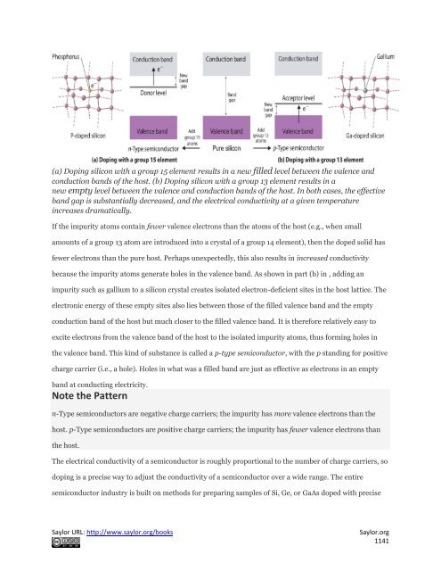
- Page 1138 and 1139: Figure 12.25 A Comparison of the Ke
- Page 1142 and 1143: amounts of desired impurities and a
- Page 1144 and 1145: a. Predict the electrical propertie
- Page 1146 and 1147: 7. Carbon is an insulator, and sili
- Page 1148 and 1149: The superconducting transition temp
- Page 1150 and 1151: superconducting at temperatures as
- Page 1152 and 1153: Compound Tc (K) YBa2Cu3O7−x 95 Bi
- Page 1154 and 1155: Formation", polymerization is the p
- Page 1156 and 1157: Many of the synthetic polymers we u
- Page 1158 and 1159: strong, and impact resistant. Its p
- Page 1160 and 1161: percentage of iron in wings and fus
- Page 1162 and 1163: SiCl4 s ( ) + 4CH 3CH 2OH ( l) + 4N
- Page 1164 and 1165: Figure 12.34 Some Possible Arrangem
- Page 1166 and 1167: Determine under what conditions the
- Page 1168 and 1169: a. Explain why the emitted light sh
- Page 1170 and 1171: 9. A polymerization reaction is use
- Page 1172 and 1173: L E A R N I N G O B JE C T I V E 1.
- Page 1174 and 1175: Solvation can be an exothermic or e
- Page 1176 and 1177: All spontaneous processes with ΔH
- Page 1178 and 1179: The first substance, LiCl, is an io
- Page 1180 and 1181: The magnitude of the changes in bot
- Page 1182 and 1183: the molecule or ion happens to coll
- Page 1184 and 1185: sodium halides increase from NaI to
- Page 1186 and 1187: Gas Solubility (M) × 10 −4 Xe 50
- Page 1188 and 1189: Low-molecular-mass hydrocarbons wit
- Page 1190 and 1191:
Exercise Identify the most importan
- Page 1192 and 1193:
E X A M P L E 3 The following subst
- Page 1194 and 1195:
solution has two or more phases tha
- Page 1196 and 1197:
(a) The potassium complex of the cr
- Page 1198 and 1199:
a. cyclohexane or methanol b. I 2 o
- Page 1200 and 1201:
A N S W E R S 1. 2. 3. 4. 5. 6. 7.
- Page 1202 and 1203:
a. A The molarity is the number of
- Page 1204 and 1205:
E X A M P L E 5 Several years ago,
- Page 1206 and 1207:
Unit Definition Application percent
- Page 1208 and 1209:
d. MEtOH = (0.686 mol100 mL) \ (100
- Page 1210 and 1211:
1. Complete the following table for
- Page 1212 and 1213:
2Fe(s) + 3Br 2 (aq) → 2FeBr 3 (aq
- Page 1214 and 1215:
1. To understand the relationship a
- Page 1216 and 1217:
process (ΔHsoln < 0). Conversely,
- Page 1218 and 1219:
"Energy Sources and the Environment
- Page 1220 and 1221:
the Henry’s law constants for sol
- Page 1222 and 1223:
CO2 = kPO2 = (1.27 ´10 - 3 M / atm
- Page 1224 and 1225:
2. The solubility of O 2 in 100 g o
- Page 1226 and 1227:
(CH3CO2Na) and 50 g of KBr, we can
- Page 1228 and 1229:
ut calcium carbonate (CaCO3) is qui
- Page 1230 and 1231:
Properties of Liquids".) (b) Increa
- Page 1232 and 1233:
The Henry’s law constant for O 2
- Page 1234 and 1235:
pump. Filling the flask with nitrog
- Page 1236 and 1237:
Solubility may increase or decrease
- Page 1238 and 1239:
decrease with increasing temperatur
- Page 1240 and 1241:
External pressure has very little e
- Page 1242 and 1243:
Note the Pattern Gases that react w
- Page 1244 and 1245:
CONCEP TUAL PROBLEMS 1. Use the kin
- Page 1246 and 1247:
L E A R N I N G O B JE C T I V E 1.
- Page 1248 and 1249:
to tissues. In a common inherited d
- Page 1250 and 1251:
(a) Soaps and detergents, which con
- Page 1252 and 1253:
hydrophobic tails attached to a hyd
- Page 1254 and 1255:
must be better.” Instead of using
- Page 1256 and 1257:
Chemical Kinetics The gases, liquid
- Page 1258 and 1259:
At 180°C, however, a completely di
- Page 1260 and 1261:
Factors that influence the reaction
- Page 1262 and 1263:
The progress of a simple reaction (
- Page 1264 and 1265:
Time (h) [Aspirin] (M) [Salicylic A
- Page 1266 and 1267:
depend on the total volume of the s
- Page 1268 and 1269:
A Using the equations in Example 1,
- Page 1270 and 1271:
eactants ([R]) after a given amount
- Page 1272 and 1273:
eaction rate of the hydrolysis reac
- Page 1274 and 1275:
C Because the reaction rate is inde
- Page 1276 and 1277:
5. During the hydrolysis reaction A
- Page 1278 and 1279:
eaction order are described in this
- Page 1280 and 1281:
This graph shows the concentrations
- Page 1282 and 1283:
In a first-order reaction, the reac
- Page 1284 and 1285:
The rate law and reaction order of
- Page 1286 and 1287:
Data for the reaction at 320°C are
- Page 1288 and 1289:
A Having been given the initial con
- Page 1290 and 1291:
synthesis of drugs. Like the first-
- Page 1292 and 1293:
At high temperatures, nitrogen diox
- Page 1294 and 1295:
1[NO2]3600 = 1[NO2]0 + kt = 10.056
- Page 1296 and 1297:
8.5 ´10 - 3 M / min34 ´10 - 3 M /
- Page 1298 and 1299:
The peroxydisulfate ion (S 2O 8 2
- Page 1300 and 1301:
C 3 H 7 Br + S 2 O 3 2− → C 3 H
- Page 1302 and 1303:
These plots show the decomposition
- Page 1304 and 1305:
E X AM P L E 9 Dinitrogen pentoxide
- Page 1306 and 1307:
second order in C 4H 6; rate = k[C
- Page 1308 and 1309:
Time (s) Pressure (mmHg) 0 348 400
- Page 1310 and 1311:
experimentally. (To understand why,
- Page 1312 and 1313:
Rate-determining step. The phenomen
- Page 1314 and 1315:
This mechanism is consistent with t
- Page 1316 and 1317:
CH3· + CH3· → H3CCH3 Cl· + Cl
- Page 1318 and 1319:
3. Nitramide (O 2 NNH 2 ) decompose
- Page 1320 and 1321:
The reaction rate, not the rate con
- Page 1322 and 1323:
The diagram shows how the energy of
- Page 1324 and 1325:
Most collisions of NO and O3 molecu
- Page 1326 and 1327:
The frequency factor is used to con
- Page 1328 and 1329:
B If the activation energy of a rea
- Page 1330 and 1331:
K E Y T A K E A W A Y For a chemic
- Page 1332 and 1333:
6. The reaction rate at 25°C is 1.
- Page 1334 and 1335:
An example of heterogeneous catalys
- Page 1336 and 1337:
Commercial Process Catalyst Reactan
- Page 1338 and 1339:
6. An area of intensive chemical re
- Page 1340 and 1341:
substrate concentrations, the plot
- Page 1342 and 1343:
9. ♦ L-Aspartic acid is an amino
- Page 1344 and 1345:
13. Figure 14.27 "Hydrogenation of
- Page 1346 and 1347:
the ratio of the reaction rate of t
- Page 1348 and 1349:
Chemical Equilibrium In Chapter 14
- Page 1350 and 1351:
(a) Initially, this idealized syste
- Page 1352 and 1353:
Given: three reaction systems Asked
- Page 1354 and 1355:
1. To know the relationship between
- Page 1356 and 1357:
K = [ C]c[ D]d[ A]a[ B]b where K is
- Page 1358 and 1359:
corresponds to an essentially irrev
- Page 1360 and 1361:
Use the value of the equilibrium co
- Page 1362 and 1363:
K¢¢ = [N2O4]1/ 2[NO2] The values
- Page 1364 and 1365:
where K is the equilibrium constant
- Page 1366 and 1367:
Incorporating all the constant valu
- Page 1368 and 1369:
Note the Pattern The concentrations
- Page 1370 and 1371:
18S8( s) +O2( g) SO2( g) K1= 4.4 ´
- Page 1372 and 1373:
A more complex example of this type
- Page 1374 and 1375:
chemical equation for the reaction,
- Page 1376 and 1377:
D We sum the numbers in the [NOCl]
- Page 1378 and 1379:
The water-gas shift reaction is imp
- Page 1380 and 1381:
K = 54 at 425°C. If 0.172 M H 2 an
- Page 1382 and 1383:
In many situations it is not necess
- Page 1384 and 1385:
100% to completion. When we solve t
- Page 1386 and 1387:
quantities or concentrations of the
- Page 1388 and 1389:
the reaction quotient is defined as
- Page 1390 and 1391:
Saylor URL: http://www.saylor.org/b
- Page 1392 and 1393:
Because K = 2.4 × 10 −4 , we see
- Page 1394 and 1395:
Initially the concentration of CO2(
- Page 1396 and 1397:
concentration of either HI or NH3,
- Page 1398 and 1399:
a. Because HgO(s) and Hg(l) are pur
- Page 1400 and 1401:
a. K = [CH 4][H 2S]2[CS2][H 2]4; ]
- Page 1402 and 1403:
1. To predict the effects of stress
- Page 1404 and 1405:
and the system will once again be a
- Page 1406 and 1407:
Exercise For each equilibrium syste
- Page 1408 and 1409:
c. 2NO2( g) 2NO( g) +O2( g) Given:
- Page 1410 and 1411:
Increasing the temperature (adding
- Page 1412 and 1413:
eaction with an unfavorable equilib
- Page 1414 and 1415:
the magnitudes of the two equilibri
- Page 1416 and 1417:
CH4 O2 CO2 H2O Q K remove water 0.6
- Page 1418 and 1419:
eaction mixture to NH3, as is done
- Page 1420 and 1421:
Controlling the amount of product f
- Page 1422 and 1423:
3. What effect does a catalyst have
- Page 1424 and 1425:
Thus we can obtain the solutions to
- Page 1426 and 1427:
3. ♦ Phosphorus pentachloride, an
- Page 1428 and 1429:
ecycling industry as well as in the
- Page 1430 and 1431:
c. Would an increase in pressure fa
- Page 1432 and 1433:
7. 8. 9. a. 10. 11. 1. K = [CO2]4[S
- Page 1434 and 1435:
definition you use. In practice, ch
- Page 1436 and 1437:
In pure water, the concentrations o
- Page 1438 and 1439:
As pH decreases, [H + ] and the aci
- Page 1440 and 1441:
Equation 16.10: [H + ] = 10 −pH D
- Page 1442 and 1443:
a. household bleach (11.4) b. milk
- Page 1444 and 1445:
ase. Once again, we have two conjug
- Page 1446 and 1447:
As we noted earlier, the concentrat
- Page 1448 and 1449:
CN - ( aq) + H2O( l) OH - ( aq) + H
- Page 1450 and 1451:
In an acid-base reaction, the proto
- Page 1452 and 1453:
You will notice in Table 16.2 "Valu
- Page 1454 and 1455:
The hydrogen sulfate ion (HSO4 −
- Page 1456 and 1457:
a. H2O( l) + HS -( aq) OH -( aq) +
- Page 1458 and 1459:
25°C is 5.13 or 3.12, respectively
- Page 1460 and 1461:
The contours show the electron dens
- Page 1462 and 1463:
B In contrast, SO 4 2− is the con
- Page 1464 and 1465:
c. C3H 7NO2( aq) +OH - ( aq) C3H6NO
- Page 1466 and 1467:
2. Arrange these bases in order of
- Page 1468 and 1469:
The same trend is predicted by anal
- Page 1470 and 1471:
These electrostatic potential maps
- Page 1472 and 1473:
causes electrons to be drawn from o
- Page 1474 and 1475:
Given: series of compounds Asked fo
- Page 1476 and 1477:
Inductive effects and charge deloca
- Page 1478 and 1479:
Equation 16.38 CCH 3CO2H = [CH 3CO2
- Page 1480 and 1481:
+(+0.0042 M ) = 0.0042 M[H +]f = [H
- Page 1482 and 1483:
H2O( l) + NH 3( aq) NH 4 + ( aq) +O
- Page 1484 and 1485:
Ka = [H+][HCO2-][HCO2H] = (1.00 ´1
- Page 1486 and 1487:
B To calculate the pH, we need to d
- Page 1488 and 1489:
As shown here for benzoic acid (C6H
- Page 1490 and 1491:
f. percent ionized = [PhCO2-]CPhCO2
- Page 1492 and 1493:
Equation 16.48 acidbasesumHA H + +A
- Page 1494 and 1495:
e determined, as can the pH of the
- Page 1496 and 1497:
8. The pK a of Cl 3 CCO 2 H is 0.64
- Page 1498 and 1499:
50.00 mL of distilled water, the pH
- Page 1500 and 1501:
As shown in part (b) in Figure 16.1
- Page 1502 and 1503:
of the titration. Note also that th
- Page 1504 and 1505:
All problems of this type must be s
- Page 1506 and 1507:
C If excess acetate is present afte
- Page 1508 and 1509:
weaker (its pKa or pKb becomes larg
- Page 1510 and 1511:
The curve for the titration of 25.0
- Page 1512 and 1513:
B The equilibrium between the weak
- Page 1514 and 1515:
Red cabbage juice contains a mixtur
- Page 1516 and 1517:
The graph shows the results obtaine
- Page 1518 and 1519:
3. The pK a values of phenol red, b
- Page 1520 and 1521:
. A volume of 5.0 mL of 2.55 M NaOH
- Page 1522 and 1523:
A N S W E R S 1. 2. 3. 43 mL 4. 5.
- Page 1524 and 1525:
changed; the ionization constant Ka
- Page 1526 and 1527:
HCO2H ( aq) H + ( aq) + HCO2 -( aq)
- Page 1528 and 1529:
A buffer maintains a relatively con
- Page 1530 and 1531:
Solution: a. According to the Hende
- Page 1532 and 1533:
[HCO2 − ] [H + ] [HCO2H] initial
- Page 1534 and 1535:
lower the final pH to 1.32 instead
- Page 1536 and 1537:
Adding Equation 16.63 and Equation
- Page 1538 and 1539:
K E Y T A K E A W A Y The common i
- Page 1540 and 1541:
d. Buffer; the NaOH neutralizes onl
- Page 1542 and 1543:
To understand how buffers work, let
- Page 1544 and 1545:
The initial concentrations, the cha
- Page 1546 and 1547:
If the equilibrium constant for the
- Page 1548 and 1549:
constant expression provides an eas
- Page 1550 and 1551:
Answer: a. 4.08 b. 9.68 The Henders
- Page 1552 and 1553:
[HCO2H] [OH − ] [HCO2 − ] initi
- Page 1554 and 1555:
weak acid; at the upper right, the
- Page 1556 and 1557:
According to Equation 16.65, adding
- Page 1558 and 1559:
d. mixing 100 mL of 0.1 M hydrofluo
- Page 1560 and 1561:
d. What is the final pH if 10.00 mL
- Page 1562 and 1563:
5. ♦ Fluoroacetic acid is a poiso
- Page 1564 and 1565:
calcium phosphate, one of the two m
- Page 1566 and 1567:
B Convert the solubility of the sal
- Page 1568 and 1569:
Asked for: molar concentration and
- Page 1570 and 1571:
If Q is less than Ksp, the solution
- Page 1572 and 1573:
continue to precipitate until the s
- Page 1574 and 1575:
The equilibrium constant for a diss
- Page 1576 and 1577:
c. iron(II) carbonate d. silver pho
- Page 1578 and 1579:
19. Use the data in Chapter 26 "App
- Page 1580 and 1581:
L E A R N I N G O B JE C T I V E 1.
- Page 1582 and 1583:
magnitude of attractive electrostat
- Page 1584 and 1585:
Ion-pair formation, the incomplete
- Page 1586 and 1587:
[Cu(NH3)4(H2O)2] 2+ complex ion is
- Page 1588 and 1589:
The value of x indicates that our a
- Page 1590 and 1591:
a. in pure water b. in 1.0 M KCl so
- Page 1592 and 1593:
detergents prevents the magnesium a
- Page 1594 and 1595:
Figure 17.5 An MRI Image of the Hea
- Page 1596 and 1597:
Equation 17.13 MA s ( ) M + ( aq) +
- Page 1598 and 1599:
(HO 2CCO 2H), which is a weak dipro
- Page 1600 and 1601:
table. Oxides of metallic elements
- Page 1602 and 1603:
elements are acidic oxides, which e
- Page 1604 and 1605:
H 2S aq ( ) H + ( aq) + HS - ( aq)H
- Page 1606 and 1607:
Substituting the desired oxalate co
- Page 1608 and 1609:
2. 3. No; both metal ions will prec
- Page 1610 and 1611:
in Chapter 6 "The Structure of Atom
- Page 1612 and 1613:
sample of AuCl, what is the solubil
- Page 1614 and 1615:
7. No; these cations would precipit
- Page 1616 and 1617:
absorbing heat—the flow of therma
- Page 1618 and 1619:
Using a frictionless piston, if the
- Page 1620 and 1621:
the engine chamber and the expandin
- Page 1622 and 1623:
Answer: −0.500 L·atm, or −50.7
- Page 1624 and 1625:
. How much work is done if the pers
- Page 1626 and 1627:
useful work is not fixed, as discus
- Page 1628 and 1629:
Equation 18.10 qp = DE + PDVconstan
- Page 1630 and 1631:
For reactions that result in a net
- Page 1632 and 1633:
. Assuming the heat capacity of the
- Page 1634 and 1635:
at a value between the initial temp
- Page 1636 and 1637:
for a Sample of Four Gas Molecules
- Page 1638 and 1639:
structure of water, leading to an i
- Page 1640 and 1641:
can continue indefinitely. In contr
- Page 1642 and 1643:
In the initial state (top), the tem
- Page 1644 and 1645:
In this case, ΔSfus = (6.01 kJ/mol
- Page 1646 and 1647:
a. What is ΔS for this process? b.
- Page 1648 and 1649:
. irreversible c. reversible d. irr
- Page 1650 and 1651:
only system that meets this criteri
- Page 1652 and 1653:
Substance S° [J/(mol·K)] CH3OH 12
- Page 1654 and 1655:
To calculate ΔS° for a chemical r
- Page 1656 and 1657:
Thus we can use a combination of he
- Page 1658 and 1659:
Entropy changes can be calculated u
- Page 1660 and 1661:
c. 114.5 J/K d. −173.2 J/K 4. 5.
- Page 1662 and 1663:
What about processes for which ΔG
- Page 1664 and 1665:
"Temperature Dependence of Δ" show
- Page 1666 and 1667:
Device Energy Conversion Approximat
- Page 1668 and 1669:
Calculate the standard free-energy
- Page 1670 and 1671:
Calculate ΔG° for the reaction of
- Page 1672 and 1673:
thermodynamically spontaneous, but
- Page 1674 and 1675:
free energy of formation (DG f ), i
- Page 1676 and 1677:
3. Nitrogen fixation is the process
- Page 1678 and 1679:
5. 919 K 6. 7. MgCO 3 : ΔG° = 63
- Page 1680 and 1681:
Because the free-energy change for
- Page 1682 and 1683:
Solution: In Example 10, we used ta
- Page 1684 and 1685:
ln K1ln K2 = -DH°RT1+ DS°R = -DH
- Page 1686 and 1687:
N U M E R I C A L PR O BL E M S 1.
- Page 1688 and 1689:
. What is the equilibrium constant
- Page 1690 and 1691:
Table 18.4 The Relationship between
- Page 1692 and 1693:
Even at 1000°C, ΔG is very positi
- Page 1694 and 1695:
B We can find the corresponding val
- Page 1696 and 1697:
Because cells are open systems, the
- Page 1698 and 1699:
information on respiration, see Cha
- Page 1700 and 1701:
Figure 18.19 NAD + and Its Reduced
- Page 1702 and 1703:
Thus any reaction that involves the
- Page 1704 and 1705:
An average 70 kg adult stores about
- Page 1706 and 1707:
A living cell is a system that is n
- Page 1708 and 1709:
a. standard enthalpy of combustion
- Page 1710 and 1711:
c. What is K? d. This reaction requ
- Page 1712 and 1713:
a. aerobic conversion b. −268 kJ
- Page 1714 and 1715:
Equation 19.1 Zn(s) + Br 2 (aq) →
- Page 1716 and 1717:
To illustrate the basic principles
- Page 1718 and 1719:
electric current can flow from the
- Page 1720 and 1721:
Answer: − a. MnO (aq) + 4 (aq) +
- Page 1722 and 1723:
The solution concentrations were no
- Page 1724 and 1725:
c. Which electrode is negatively ch
- Page 1726 and 1727:
19.2 Standard Potentials L E A R N
- Page 1728 and 1729:
an electrochemical reaction and the
- Page 1730 and 1731:
The SHE consists of platinum wire t
- Page 1732 and 1733:
E° values do not depend on the sto
- Page 1734 and 1735:
6H 2 O(l) + 2Al(s) + 2OH − (aq)
- Page 1736 and 1737:
In acidic solution, the redox react
- Page 1738 and 1739:
Equation 19.40 Zn(s)∣ Zn 2+ (aq,
- Page 1740 and 1741:
When using a galvanic cell to measu
- Page 1742 and 1743:
The voltage E′ is a constant that
- Page 1744 and 1745:
C O N C E PTUAL P R OBLEMS 1. Is a
- Page 1746 and 1747:
c. Fe 3+ (aq) + Cd(s) → Fe 2+ (aq
- Page 1748 and 1749:
1. To know how to predict the relat
- Page 1750 and 1751:
significantly greater ΔHhydration
- Page 1752 and 1753:
Answer: a. Ag + (aq); H 2O 2(aq) b.
- Page 1754 and 1755:
The oxidative and reductive strengt
- Page 1756 and 1757:
phenomenon of electrolysis and laid
- Page 1758 and 1759:
Use the data in Table 19.2 "Standar
- Page 1760 and 1761:
Thus E°cell is directly proportion
- Page 1762 and 1763:
ΔG = ΔG° + RT ln Q We also know
- Page 1764 and 1765:
Applying the Nernst equation to a s
- Page 1766 and 1767:
As the reaction progresses, the con
- Page 1768 and 1769:
Ecell = 0 V - (0.0591 V1)log([Ag+]d
- Page 1770 and 1771:
Another use for the Nernst equation
- Page 1772 and 1773:
measure the solubility product of a
- Page 1774 and 1775:
9. 10. N U M E R I C A L PR O BL E
- Page 1776 and 1777:
g. Is the reduction of Mn 3+ (aq) t
- Page 1778 and 1779:
c. What conditions can be changed t
- Page 1780 and 1781:
graphite, and starch (part (a) in F
- Page 1782 and 1783:
caused by the solid electrolyte, on
- Page 1784 and 1785:
anode: Cd(s) + 2OH − (aq) → Cd(
- Page 1786 and 1787:
When an external voltage in excess
- Page 1788 and 1789:
called an alkaline battery when ada
- Page 1790 and 1791:
deoxygenated water will not rust—
- Page 1792 and 1793:
Holes in a protective coating allow
- Page 1794 and 1795:
(Figure 19.20 "The Use of a Sacrifi
- Page 1796 and 1797:
a. Not unless you plan to sell the
- Page 1798 and 1799:
(a) When compartments that contain
- Page 1800 and 1801:
The electrolysis of a molten mixtur
- Page 1802 and 1803:
Equation 19.111 anode : 2H2O l Equa
- Page 1804 and 1805:
control its electrical conductivity
- Page 1806 and 1807:
Summary In electrolysis, an externa
- Page 1808 and 1809:
19.8 End-of-Chapter Material A P P
- Page 1810 and 1811:
when Cr(II) is oxidized to Cr(III)
- Page 1812 and 1813:
Metal E versus Ag/AgCl (V) Monel [N
- Page 1814 and 1815:
9. 10. 11. 12. 13. 14. 15. 16. 17.
- Page 1816 and 1817:
living organisms is 1.3 × 10 −12
- Page 1818 and 1819:
The relationship between the number
- Page 1820 and 1821:
hypothesis that the nucleus contain
- Page 1822 and 1823:
with 114 protons and 184 neutrons m
- Page 1824 and 1825:
3. Give the number of protons, the
- Page 1826 and 1827:
Chapter 20 Nuclear Chemistry Until
- Page 1828 and 1829:
living organisms is 1.3 × 10 −12
- Page 1830 and 1831:
Figure 20.1 Competing Interactions
- Page 1832 and 1833:
numbers 2, 8, 20, 50, 82, and 126.
- Page 1834 and 1835:
f. This nuclide has an atomic numbe
- Page 1836 and 1837:
5. Isotopes with magic numbers of p
- Page 1838 and 1839:
starting material. As we shall see,
- Page 1840 and 1841:
Similarly, the lower left subscript
- Page 1842 and 1843:
R88226a ® R86222n +a24 Because nuc
- Page 1844 and 1845:
The atomic numbers of the parent an
- Page 1846 and 1847:
a. A We know the identities of the
- Page 1848 and 1849:
a proton and an electron. The elect
- Page 1850 and 1851:
The first successful nuclear transm
- Page 1852 and 1853:
number of the target is 27, so the
- Page 1854 and 1855:
Data source: T. R. England and B. F
- Page 1856 and 1857:
charge. Six different kinds of nucl
- Page 1858 and 1859:
8. Which types of nuclear decay rea
- Page 1860 and 1861:
c. a. Ra ® R86220n +a 208 Tl → 8
- Page 1862 and 1863:
a. An unknown element emits γ rays
- Page 1864 and 1865:
ays, their interaction with matter
- Page 1866 and 1867:
the rem (roentgen equivalent in man
- Page 1868 and 1869:
By far the most important source of
- Page 1870 and 1871:
adiation dose per year = 2.87 ´10
- Page 1872 and 1873:
Studies on fruit flies show a linea
- Page 1874 and 1875:
1. 2. 3. Ionizing radiation is high
- Page 1876 and 1877:
Equation 20.29 DE = (Dm)c2 we can r
- Page 1878 and 1879:
A Using particle and isotope masses
- Page 1880 and 1881:
smooth curve but exhibits sharp pea
- Page 1882 and 1883:
Nuclear Fission and Fusion First di
- Page 1884 and 1885:
Figure 20.18 Nuclear Fusion In a nu
- Page 1886 and 1887:
DE = (-0.188386 amu)(931 MeV / amu)
- Page 1888 and 1889:
a. 4. a. P91234a ® ?+ b -10 b. R88
- Page 1890 and 1891:
. The formation of lead-206 by alph
- Page 1892 and 1893:
an uncontrolled nuclear chain react
- Page 1894 and 1895:
neutrons, slowing them to increase
- Page 1896 and 1897:
eactor to produce twice as much fis
- Page 1898 and 1899:
or the kidneys, which are almost in
- Page 1900 and 1901:
shown in Figure 20.25 "Using Radiat
- Page 1902 and 1903:
1. Neutron flow is regulated by usi
- Page 1904 and 1905:
some examples are Ru and Ir. You ma
- Page 1906 and 1907:
heavier elements such as carbon and
- Page 1908 and 1909:
concentration of neutrons is so gre
- Page 1910 and 1911:
4. During the lifetime of a star, d
- Page 1912 and 1913:
Neglecting the fission products, wr
- Page 1914 and 1915:
12. 130 W 13. Saylor URL: http://ww
- Page 1916 and 1917:
to lose electrons in chemical react
- Page 1918 and 1919:
C to C bonds are common for carbon,
- Page 1920 and 1921:
c. predict which element differs th
- Page 1922 and 1923:
C O N C E PTUAL P R OBLEMS 1. List
- Page 1924 and 1925:
S T R U C T U R E A N D R E A C T I
- Page 1926 and 1927:
Urey won the Nobel Prize in Chemist
- Page 1928 and 1929:
Because of its 1s 1 electron config
- Page 1930 and 1931:
Hydrogen gas can also be generated
- Page 1932 and 1933:
g. Pd h. Al 6. Which has the higher
- Page 1934 and 1935:
8. Seawater contains 3.5% dissolved
- Page 1936 and 1937:
sulfuric acid to dissolve the desir
- Page 1938 and 1939:
product of reaction with Lithium So
- Page 1940 and 1941:
Equation 21.10 4KO 2 (s) + 2CO 2 (g
- Page 1942 and 1943:
stoichiometry and color of intercal
- Page 1944 and 1945:
"Solutions", crown ethers are cycli
- Page 1946 and 1947:
Figure 21.11 Alkali Metal-Liquid Am
- Page 1948 and 1949:
esponsible for transmitting nerve i
- Page 1950 and 1951:
d. Li 3N(s) + KCl(s) → Given: rea
- Page 1952 and 1953:
to form ionic halides; the heavier
- Page 1954 and 1955:
3. Sodium metal is prepared by elec
- Page 1956 and 1957:
The alkaline earth metals are produ
- Page 1958 and 1959:
One major difference between the gr
- Page 1960 and 1961:
The reaction in Equation 21.27 is t
- Page 1962 and 1963:
Organometallic Compounds Containing
- Page 1964 and 1965:
whereas that of BaCO 3 is almost tw
- Page 1966 and 1967:
must appear in the products, and bo
- Page 1968 and 1969:
1. Beryllium iodide reacts vigorous
- Page 1970 and 1971:
L E A R N I N G O B JE C T I V E 1.
- Page 1972 and 1973:
containing structural materials. No
- Page 1974 and 1975:
Because the health of cells depends
- Page 1976 and 1977:
Summary Covalent hydrides in which
- Page 1978 and 1979:
2. Ultrahigh-purity tritium, which
- Page 1980 and 1981:
cell. The Na + , K + , Mg 2+ , and
- Page 1982 and 1983:
1. To understand the trends in prop
- Page 1984 and 1985:
group 13 elements, only aluminum is
- Page 1986 and 1987:
Property Boron Aluminum* Gallium In
- Page 1988 and 1989:
Unlike metallic solids, elemental b
- Page 1990 and 1991:
(a) The hydrogen-bridged dimer B2H6
- Page 1992 and 1993:
oxidized to H + and O 2 will be red
- Page 1994 and 1995:
in dilute acid, but Al2O3 and Ga2O3
- Page 1996 and 1997:
Because Al is a main group element
- Page 1998 and 1999:
7. Because the B-N unit is isoelect
- Page 2000 and 2001:
d. B 2 H 6 (g) + 2(C 2 H 5 ) 2 S(g)
- Page 2002 and 2003:
d. 16Ga(l) + 3S 8 (s) → 8Ga 2 S 3
- Page 2004 and 2005:
The most common sources of diamonds
- Page 2006 and 2007:
stoichiometry as those of carbon, h
- Page 2008 and 2009:
laboratory, fullerenes have been fo
- Page 2010 and 2011:
temperatures with electropositive m
- Page 2012 and 2013:
Predict the products of the reactio
- Page 2014 and 2015:
Silicon has relatively low-energy,
- Page 2016 and 2017:
The cavities normally contain hydra
- Page 2018 and 2019:
The structure of a linear silicone
- Page 2020 and 2021:
character increases. Silicates cont
- Page 2022 and 2023:
22.3 The Elements of Group 15 (The
- Page 2024 and 2025:
about 0.1% of Earth’s crust, is m
- Page 2026 and 2027:
Note the Pattern Because neutral co
- Page 2028 and 2029:
About 10% of the ammonia produced a
- Page 2030 and 2031:
to handle. A third allotrope of pho
- Page 2032 and 2033:
The heavier pnicogens form sulfides
- Page 2034 and 2035:
states. The stability of the +5 oxi
- Page 2036 and 2037:
A N S W E R S 1. 2. 3. 4. 5. NaNO 2
- Page 2038 and 2039:
photosensitive, selenium is also us
- Page 2040 and 2041:
selenium) have similar properties b
- Page 2042 and 2043:
covalent compounds in which the bon
- Page 2044 and 2045:
Because most of the heavier chalcog
- Page 2046 and 2047:
contain C=S or C=Se bonds and have
- Page 2048 and 2049:
Summary Because the electronegativi
- Page 2050 and 2051:
4. 5. CrO 3 < Al 2 O 3 < Sc 2 O 3 <
- Page 2052 and 2053:
the Cl2 produced annually; organobr
- Page 2054 and 2055:
Oxidative strength decreases down g
- Page 2056 and 2057:
covalent character of the halide du
- Page 2058 and 2059:
a. When the reactants have the same
- Page 2060 and 2061:
2. 3. 4. 5. Ionic character decreas
- Page 2062 and 2063:
was the first of the noble gases to
- Page 2064 and 2065:
Property Helium Neon Argon Krypton
- Page 2066 and 2067:
Xe(g) + 2F 2 (g) → XeF 4 (s) The
- Page 2068 and 2069:
Based on the position of radon in t
- Page 2070 and 2071:
2. Write a balanced chemical equati
- Page 2072 and 2073:
d. the reactivity of elemental C an
- Page 2074 and 2075:
20. Zeolites have become increasing
- Page 2076 and 2077:
Chapter 23 The d-Block Elements Cha
- Page 2078 and 2079:
Because of the lanthanide contracti
- Page 2080 and 2081:
Due to a small increase in successi
- Page 2082 and 2083:
Sc Ti V Cr Mn Fe Co Ni Cu Zn V V V
- Page 2084 and 2085:
Most transition-metal compounds are
- Page 2086 and 2087:
The group 3 metals react with nonme
- Page 2088 and 2089:
Each titanium atom is surrounded by
- Page 2090 and 2091:
molybdenum produced annually is use
- Page 2092 and 2093:
engines. Because tungsten itself ha
- Page 2094 and 2095:
discovered until the 19th century.
- Page 2096 and 2097:
The groups 8-10 metals form a range
- Page 2098 and 2099:
dissolves in the 3:1 HCl:HNO3 mixtu
- Page 2100 and 2101:
Refer to the periodic trends in thi
- Page 2102 and 2103:
adius ratio causes extensive polari
- Page 2104 and 2105:
4. Most of the transition metals ca
- Page 2106 and 2107:
1. 2. 3. 4. 5. 6. 7. 8. 9. Pt 10+ ,
- Page 2108 and 2109:
2FeTiO 3 (s) + 6C(s) + 7Cl 2 (g)
- Page 2110 and 2111:
on sulfuric acid production, see Ch
- Page 2112 and 2113:
Group Element Z Valence Electron Co
- Page 2114 and 2115:
All three group 7 elements have sev
- Page 2116 and 2117:
nickel uses the same alloy. In cont
- Page 2118 and 2119:
old. Copper is almost as ancient, w
- Page 2120 and 2121:
atteries. Large amounts of mercury
- Page 2122 and 2123:
chlorine. The most likely combinati
- Page 2124 and 2125:
group 8 metals in their highest oxi
- Page 2126 and 2127:
9. Pt 10+ , Ir 9+ , and Ni 10+ . Be
- Page 2128 and 2129:
Equation 23.5 PbS s ( ) + O2( g) ®
- Page 2130 and 2131:
WO3( s) +3H2( g)- ® DW ( s) +3H2O(
- Page 2132 and 2133:
2. 3. VCl4 l ( ) +2H 2( g)VCl4( l)
- Page 2134 and 2135:
present. For example, Werner’s da
- Page 2136 and 2137:
MA 4B 2 complexes with each of the
- Page 2138 and 2139:
Coordination Number 2 Although it i
- Page 2140 and 2141:
This coordination number is by far
- Page 2142 and 2143:
ases are hard acids, whereas metal
- Page 2144 and 2145:
Experimentally, it is observed that
- Page 2146 and 2147:
Isomers that contain the same numbe
- Page 2148 and 2149:
Octahedral complexes also exhibit c
- Page 2150 and 2151:
In addition, two structures are pos
- Page 2152 and 2153:
2. Can a tetrahedral MA 2 B 2 compl
- Page 2154 and 2155:
ligands like CO, CFT enables chemis
- Page 2156 and 2157:
(Crystal field splitting energy als
- Page 2158 and 2159:
magnitude of Δo depends on three f
- Page 2160 and 2161:
Note the Pattern The largest Δos a
- Page 2162 and 2163:
spin d 6 complexes, which accounts
- Page 2164 and 2165:
energy is not the same for all five
- Page 2166 and 2167:
D In a high-spin octahedral d 6 com
- Page 2168 and 2169:
line represents the behavior predic
- Page 2170 and 2171:
Figure 23.16 The Jahn-Teller Effect
- Page 2172 and 2173:
Values of the lattice energies for
- Page 2174 and 2175:
4. The ionic radii of V 2+ , Fe 2+
- Page 2176 and 2177:
Consequently, most microorganisms s
- Page 2178 and 2179:
A schematic drawing of the structur
- Page 2180 and 2181:
(−0.20 to −0.50 V) potentials,
- Page 2182 and 2183:
lue copper protein. Moreover, the r
- Page 2184 and 2185:
In a cytochrome c, the heme iron is
- Page 2186 and 2187:
transport system is available to pr
- Page 2188 and 2189:
(a) The Fe 2+ ion in deoxymyoglobin
- Page 2190 and 2191:
electron density is so great that t
- Page 2192 and 2193:
Although hemocyanin and hemerythrin
- Page 2194 and 2195:
The active site of carbonic anhydra
- Page 2196 and 2197:
In the conversion of ethylene glyco
- Page 2198 and 2199:
2. Gout is a painful disorder cause
- Page 2200 and 2201:
these complexes is octahedral; in t
- Page 2202 and 2203:
(carboxylate-bridged copper dimers)
- Page 2204 and 2205:
Figure 24.1 Major Classes of Organi
- Page 2206 and 2207:
positions of groups attached to an
- Page 2208 and 2209:
Figure 24.3 Carbon-Carbon Bonding i
- Page 2210 and 2211:
Figure 24.5 Potential Energy Plot a
- Page 2212 and 2213:
Structural Isomers Unlike conformat
- Page 2214 and 2215:
E X A M P L E 2 Draw all the struct
- Page 2216 and 2217:
superimposed on its mirror image, a
- Page 2218 and 2219:
E X A M P L E 3 Draw the cis and tr
- Page 2220 and 2221:
. 1-methyl-3-chlorocyclopentane Ans
- Page 2222 and 2223:
Although enantiomers have identical
- Page 2224 and 2225:
physical and chemical properties, w
- Page 2226 and 2227:
pregnancy, but unfortunately only t
- Page 2228 and 2229:
A N S W E R S 1. sp 3 ; it is a σ
- Page 2230 and 2231:
a. Draw the structures of the enant
- Page 2232 and 2233:
24.3 Reactivity of Organic Molecule
- Page 2234 and 2235:
Adding one electron to a carbocatio
- Page 2236 and 2237:
c. The (CH 3) 3C + cation contains
- Page 2238 and 2239:
c. (CH 3 ) 3 N + BCl 3 → 24.4 Com
- Page 2240 and 2241:
Some reactions involve the removal,
- Page 2242 and 2243:
Equation 24.6 Br ×+ Br ×CH 3CH 2
- Page 2244 and 2245:
a. The CN − ion of KCN is a poten
- Page 2246 and 2247:
2. Sketch the mechanism for the nuc
- Page 2248 and 2249:
the solid state. It is therefore se
- Page 2250 and 2251:
Saylor URL: http://www.saylor.org/b
- Page 2252 and 2253:
Alkenes and alkynes are most often
- Page 2254 and 2255:
carbocation formed in the first ste
- Page 2256 and 2257:
Oxygen- and Nitrogen-Containing Fun
- Page 2258 and 2259:
In compounds containing a carbonyl
- Page 2260 and 2261:
Containing Functional Groups"), and
- Page 2262 and 2263:
Compounds that contain the carboxyl
- Page 2264 and 2265:
protonate the doubly bonded oxygen
- Page 2266 and 2267:
the two substituents on the amide n
- Page 2268 and 2269:
onded to one hydrogen and two alkyl
- Page 2270 and 2271:
Given: reactants Asked for: product
- Page 2272 and 2273:
substitution reaction. Alcohols und
- Page 2274 and 2275:
A N S W E R S 1. 2. 3. 4. 5. (c) an
- Page 2276 and 2277:
1. To understand the general proper
- Page 2278 and 2279:
In contrast, the radicals formed du
- Page 2280 and 2281:
Alkenes and alkynes are most often
- Page 2282 and 2283:
The carbocation formed in the first
- Page 2284 and 2285:
contain the carbonyl functional gro
- Page 2286 and 2287:
Figure 24.17 Some Familiar Aldehyde
- Page 2288 and 2289:
Containing Functional Groups"), and
- Page 2290 and 2291:
Compounds that contain the carboxyl
- Page 2292 and 2293:
protonate the doubly bonded oxygen
- Page 2294 and 2295:
the two substituents on the amide n
- Page 2296 and 2297:
molecular masses. Primary amines te
- Page 2298 and 2299:
Solution: a. The proton on the carb
- Page 2300 and 2301:
density. An alcohol is often prepar
- Page 2302 and 2303:
15. What factors determine the reac
- Page 2304 and 2305:
24.6 The Molecules of Life L E A R
- Page 2306 and 2307:
In solution, simple sugars exist pr
- Page 2308 and 2309:
Because carbohydrates have a carbon
- Page 2310 and 2311:
Given: Fischer projection of a suga
- Page 2312 and 2313:
The double bonds of unsaturated fat
- Page 2314 and 2315:
Nucleic Acids Nucleic acids are the
- Page 2316 and 2317:
untreated, it produces severe brain
- Page 2318 and 2319:
2. Cyclohexanecarboxylic acid is a
- Page 2320 and 2321:
Both glyceraldehyde and glyceric ac
- Page 2322 and 2323:
1. The first staggered conformation
- Page 2324 and 2325:
Substance ΔHf° (kJ/mol) ΔGf° (k
- Page 2326 and 2327:
Substance ΔHf° (kJ/mol) ΔGf° (k
- Page 2328 and 2329:
Substance ΔHf° (kJ/mol) ΔGf° (k
- Page 2330 and 2331:
Substance ΔHf° (kJ/mol) ΔGf° (k
- Page 2332 and 2333:
Substance ΔHf° (kJ/mol) ΔGf° (k
- Page 2334 and 2335:
Substance ΔHf° (kJ/mol) ΔGf° (k
- Page 2336 and 2337:
Compound Name Compound Formula K sp
- Page 2338 and 2339:
Compound Name Compound Formula K sp
- Page 2340 and 2341:
Name Formula K a1 pKa1 K a2 pKa2 K
- Page 2342 and 2343:
Chapter 27 Appendix C: Dissociation
- Page 2344 and 2345:
Name Formula K a1 pKa1 K a2 pKa2 K
- Page 2346 and 2347:
Chapter 29 Appendix E: Standard Red
- Page 2348 and 2349:
Half-Reaction E° (V) Cu 2+ + 2e
- Page 2350 and 2351:
Half-Reaction E° (V) Nd 3+ + 3e
- Page 2352 and 2353:
Half-Reaction E° (V) U 3+ + 3e −
- Page 2354 and 2355:
10 1.2281 40 7.3814 70 31.176 100 1
- Page 2356 and 2357:
Chapter 32 Appendix H: Periodic Tab
- Page 2358 and 2359:
List of Elements Name Symbol Atomic
- Page 2360 and 2361:
List of Elements Name Symbol Atomic
- Page 2362 and 2363:
Chapter 33 Appendix I: Experimental
- Page 2364 and 2365:
Chapter 34 Art Credits 34.1 Molecul