SPIRE Design Description - Research Services
SPIRE Design Description - Research Services
SPIRE Design Description - Research Services

You also want an ePaper? Increase the reach of your titles
YUMPU automatically turns print PDFs into web optimized ePapers that Google loves.
Draft <strong>SPIRE</strong> <strong>Design</strong> <strong>Description</strong> Document<br />
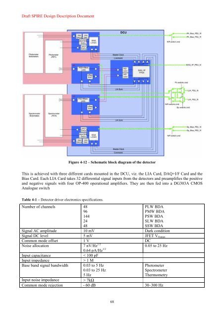
Figure 4-12 – Schematic block diagram of the detector<br />
This is achieved with three different cards mounted in the DCU, viz. the LIA Card, DAQ+I/F Card and the<br />
Bias Card. Each LIA Card takes 32 differential signal inputs from the detectors and preamplifies the positive<br />
and negative signals with four OP-400 operational amplifiers. They are then fed into a DG303A CMOS<br />
Analogue switch<br />
Table 4-1 – Detector driver electronics specifications.<br />
Number of channels 48<br />
96<br />
144<br />
24<br />
48<br />
68<br />
PLW BDA<br />
PMW BDA<br />
PSW BDA<br />
SLW BDA<br />
SSW BDA<br />
Signal AC amplitude 10 mV Dark condition<br />
Signal DC level 5 mV JFET VOsmax<br />
Common mode offset 1 V DC<br />
Noise allocation 7 nV/Hz 1/2<br />
0.64 pA/Hz 1/2<br />
0.05 to 25 Hz<br />
Input capacitance < 100 pF<br />
Input impedance > 1 M<br />
Base band signal bandwidth 0.03 to 5 Hz<br />
Photometer<br />
0.03 to 25 Hz<br />
Spectrometer<br />
5 Hz<br />
Thermometry<br />
Input noise impedance > 7kΩ<br />
Common mode rejection - 60 dB 30–300 Hz