PDF version - ARM Information Center
PDF version - ARM Information Center
PDF version - ARM Information Center

Create successful ePaper yourself
Turn your PDF publications into a flip-book with our unique Google optimized e-Paper software.
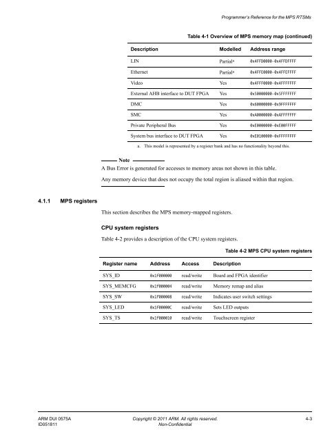
Programmer’s Reference for the MPS RTSMsTable 4-1 Overview of MPS memory map (continued)Description Modelled Address rangeLIN Partial a 0x4FFD0000–0x4FFDFFFFEthernet Partial a 0x4FFE0000–0x4FFEFFFFVideo Yes 0x4FFF0000–0x4FFFFFFFExternal AHB interface to DUT FPGA Yes 0x50000000–0x5FFFFFFFDMC Yes 0x60000000–0x9FFFFFFFSMC Yes 0xA0000000–0xAFFFFFFFPrivate Peripheral Bus Yes 0xE0000000–0xE00FFFFFSystem bus interface to DUT FPGA Yes 0xE0100000–0xFFFFFFFFa. This model is represented by a register bank and has no functionality beyond this.NoteA Bus Error is generated for accesses to memory areas not shown in this table.Any memory device that does not occupy the total region is aliased within that region.4.1.1 MPS registersThis section describes the MPS memory-mapped registers.CPU system registersTable 4-2 provides a description of the CPU system registers.Table 4-2 MPS CPU system registersRegister name Address Access DescriptionSYS_ID 0x1f000000 read/write Board and FPGA identifierSYS_MEMCFG 0x1f000004 read/write Memory remap and aliasSYS_SW 0x1f000008 read/write Indicates user switch settingsSYS_LED 0x1f00000C read/write Sets LED outputsSYS_TS 0x1f000010 read/write Touchscreen register<strong>ARM</strong> DUI 0575A Copyright © 2011 <strong>ARM</strong>. All rights reserved. 4-3ID051811Non-Confidential