MPhil thesis of Lo Chi Wa - Department of Electronic & Computer ...
MPhil thesis of Lo Chi Wa - Department of Electronic & Computer ...
MPhil thesis of Lo Chi Wa - Department of Electronic & Computer ...

You also want an ePaper? Increase the reach of your titles
YUMPU automatically turns print PDFs into web optimized ePapers that Google loves.
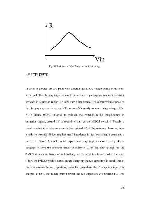
RVinFig. 38 Resistance <strong>of</strong> NMOS resistor vs. input voltageCharge pumpIn order to provide the two paths with different gains, two charge-pumps <strong>of</strong> differentsizes used. The charge-pumps are simple current steering charge-pumps with transistorswitches in saturation region for large output impedance. The output voltage range <strong>of</strong>the charge-pumps can be very small because <strong>of</strong> the nearly constant tuning voltage <strong>of</strong> theVCO, around 0.55V. In order to maintain the switches in the charge-pumps insaturation region, around 1V is needed to turn on the NMOS switches. Usually aresistive potential divider can generate the required 1V for the switches. However, sincea resistive potential divider requires small impedance for fast switching, it consumes alot <strong>of</strong> DC power. A simple switch capacitor driving stage, as shown in Fig. 40, isdesigned to drive the saturated transistor switches. When the input is high, all theNMOS switches are turned on and discharge all the capacitors to zero. When the inputis low, the PMOS switch is turned on and charge up the two capacitors in serial. Due tothe ratio between the two capacitors, when the upper electrode <strong>of</strong> the upper capacitor ischarged to 1.5V, the middle point between the two capacitors will become 1V. This53