MPhil thesis of Lo Chi Wa - Department of Electronic & Computer ...
MPhil thesis of Lo Chi Wa - Department of Electronic & Computer ...
MPhil thesis of Lo Chi Wa - Department of Electronic & Computer ...

Create successful ePaper yourself
Turn your PDF publications into a flip-book with our unique Google optimized e-Paper software.
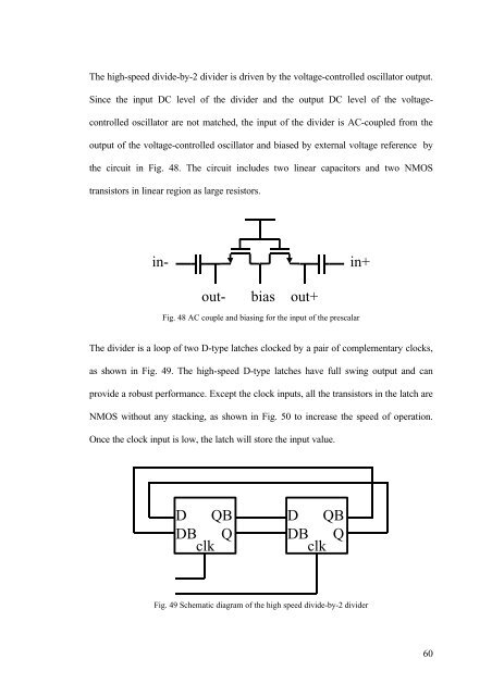
The high-speed divide-by-2 divider is driven by the voltage-controlled oscillator output.Since the input DC level <strong>of</strong> the divider and the output DC level <strong>of</strong> the voltagecontrolledoscillator are not matched, the input <strong>of</strong> the divider is AC-coupled from theoutput <strong>of</strong> the voltage-controlled oscillator and biased by external voltage reference bythe circuit in Fig. 48. The circuit includes two linear capacitors and two NMOStransistors in linear region as large resistors.in+out+out-biasin-Fig. 48 AC couple and biasing for the input <strong>of</strong> the prescalarThe divider is a loop <strong>of</strong> two D-type latches clocked by a pair <strong>of</strong> complementary clocks,as shown in Fig. 49. The high-speed D-type latches have full swing output and canprovide a robust performance. Except the clock inputs, all the transistors in the latch areNMOS without any stacking, as shown in Fig. 50 to increase the speed <strong>of</strong> operation.Once the clock input is low, the latch will store the input value.D QBDB QclkD QBDB QclkFig. 49 Schematic diagram <strong>of</strong> the high speed divide-by-2 divider60