MPhil thesis of Lo Chi Wa - Department of Electronic & Computer ...
MPhil thesis of Lo Chi Wa - Department of Electronic & Computer ...
MPhil thesis of Lo Chi Wa - Department of Electronic & Computer ...

You also want an ePaper? Increase the reach of your titles
YUMPU automatically turns print PDFs into web optimized ePapers that Google loves.
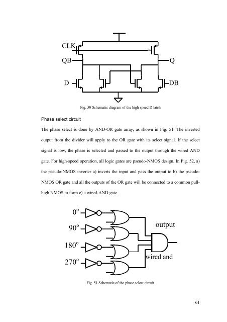
CLKQBQDDBFig. 50 Schematic diagram <strong>of</strong> the high speed D latchPhase select circuitThe phase select is done by AND-OR gate array, as shown in Fig. 51. The invertedoutput from the divider will apply to the OR gate with its select signal. If the selectsignal is low, the phase is selected and passed to the output through the wired ANDgate. For high-speed operation, all logic gates are pseudo-NMOS design. In Fig. 52, a)the pseudo-NMOS inverter a) inverts the input and pass the output to b) the pseudo-NMOS OR gate and all the outputs <strong>of</strong> the OR gate will be connected to a common pullhighNMOS to form c) a wired-AND gate.0 o90 ooutput180 owired and270 oFig. 51 Schematic <strong>of</strong> the phase select circuit61