GS1 EPC Tag Data Standard 1.6 - Indicod-Ecr
GS1 EPC Tag Data Standard 1.6 - Indicod-Ecr
GS1 EPC Tag Data Standard 1.6 - Indicod-Ecr
- No tags were found...

You also want an ePaper? Increase the reach of your titles
YUMPU automatically turns print PDFs into web optimized ePapers that Google loves.
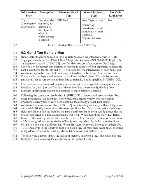
InformationTypeDescription Where on Gen 2<strong>Tag</strong>Where TypicallyUsedBar CodeEquivalent<strong>Tag</strong>ManufactureInformationDescribes thetag itself, asopposed tothe physicalobject towhich the tagis affixedTID Bank<strong>Data</strong> Capture layerUnique tagmanufacture serialnumber may reachBusinessApplication layerNo1647Table 3.Kinds of <strong>Data</strong> on a Gen 2 RFID <strong>Tag</strong>164816491650165116521653165416551656165716581659166016611662166316641665166616671668166916701671167216739.2 Gen 2 <strong>Tag</strong> Memory MapBinary data structures defined in the <strong>Tag</strong> <strong>Data</strong> <strong>Standard</strong> are intended for use in RFID<strong>Tag</strong>s, particularly in UHF Class 1 Gen 2 <strong>Tag</strong>s (also known as ISO 18000-6C <strong>Tag</strong>s). Theair interface standard [UHFC1G2] specifies the structure of memory on Gen 2 tags.Specifically, it specifies that memory in these tags consists of four separately addressablebanks, numbered 00, 01, 10, and 11. It also specifies the intended use of each bank, andconstraints upon the content of each bank dictated by the behavior of the air interface.For example, the layout and meaning of the Reserved bank (bank 00), which containspasswords that govern certain air interface commands, is fully specified in [UHFC1G2].For those memory banks and memory locations that have no special meaning to the airinterface (i.e., are “just data” as far as the air interface is concerned), the <strong>Tag</strong> <strong>Data</strong><strong>Standard</strong> specifies the content and meaning of these memory locations.Following the convention established in [UHFC1G2], memory addresses are describedusing hexadecimal bit addresses, where each bank begins with bit 00 h and extendsupward to as many bits as each bank contains, the capacity of each bank beingconstrained in some respects by [UHFC1G2] but ultimately may vary with each tag makeand model. Bit 00 h is considered the most significant bit of each bank, and when binaryfields are laid out into tag memory the most significant bit of any given field occupies thelowest-numbered bit address occupied by that field. When describing individual fields,however, the least significant bit is numbered zero. For example, the Access Password isa 32-bit unsigned integer consisting of bits b 31 b 30 …b 0 , where b 31 is the most significantbit and b 0 is the least significant bit. When the Access Password is stored at address 20 h– 3F h (inclusive) in the Reserved bank of a Gen 2 tag, the most significant bit b 31 is storedat tag address 20 h and the least significant bit b 0 is stored at address 3F h .The following diagram shows the layout of memory on a Gen 2 tag, The colors indicatethe type of data following the categorization in Section Figure 1.Copyright ©2005- 2011 <strong>GS1</strong> AISBL, All Rights Reserved. Page 55 of 218