Voltage References
Voltage References
Voltage References
You also want an ePaper? Increase the reach of your titles
YUMPU automatically turns print PDFs into web optimized ePapers that Google loves.
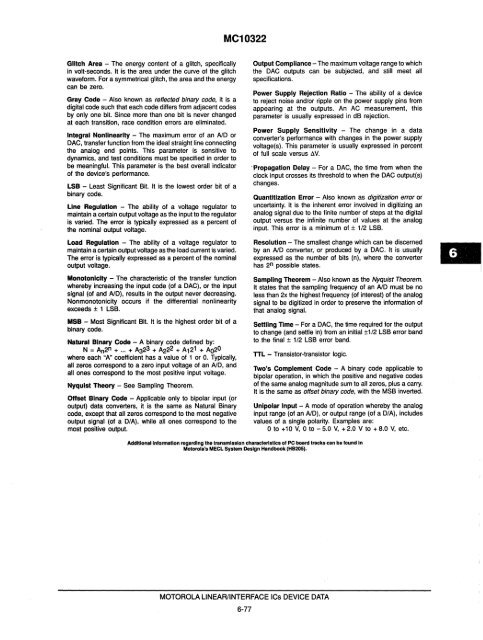
Glitch Area - The energy content of a glitch, specifically<br />
In volt-seconds. It is the area under the curve of the glitch<br />
waveform. For a symmetrical glitch, the area and the energy<br />
can be zero.<br />
Gray Code - Also known as reflected binary code, it is a<br />
digital code such that each code differs from adjacent codes<br />
by only one bit. Since more than one bit is never changed<br />
at each transition, race condition errors are eliminated.<br />
Integral Nonlinearity - The maximum error of an ND or<br />
DAC, transfer function from the ideal straight line connecting<br />
the analog end points. This parameter is sensitive to<br />
dynamics, and test conditions must be specified in order to<br />
be meaningful. This parameter is the best overall indicator<br />
of the device's performance.<br />
LSB - Least Significant Bit. It is the lowest order bit of a<br />
binary code.<br />
Line Regulation - The ability of a voltage regulator to<br />
maintain a certain output voltage as the input to the regulator<br />
is varied. The error is typically expressed as a percent of<br />
the nominal output voltage.<br />
Load Regulation - The ability of a voltage regulator to<br />
maintain a certain output voltage as the load current is varied.<br />
The error is typically expressed as a percent of the nominal<br />
output voltage.<br />
Monotonlclty - The characteristic of the transfer function<br />
whereby increasing the input code (of a DAC), or the input<br />
Signal (of and ND), results in the output never decreasing.<br />
Nonmonotonicity occurs if the differential nonlinearity<br />
exceeds ± 1 LSB.<br />
MSB - Most Significant Bit. It is the highest order bit of a<br />
binary code.<br />
Natural Binary Code - A binary code defined by:<br />
N = An2n + ... + Aa23 + A222 + A121 + A020<br />
where each "A" coefficient has a value of 1 or O. Typically,<br />
all zeros correspond to a zero input voltage of an ND, and<br />
all ones correspond to the most positive Input voltage.<br />
Nyquist Theory - See Sampling Theorem.<br />
Offset Binary Code - Applicable only to bipolar input (or<br />
output) data converters, it is the same as Natural Binary<br />
code, except that all zeros correspond to the most negative<br />
output signal (of a D/A), while all ones correspond to the<br />
most positive output. .<br />
MC10322<br />
Output Compliance - The maximum voltage range to which<br />
the DAC outputs can be subjected, and still meet all<br />
specifications.<br />
Power Supply Rejection Ratio - The ability of a device<br />
to reject noise andlor ripple on the power supply pins from<br />
appearing at the outputs. An AC measurement, this<br />
parameter is usually expressed in dB rejection.<br />
Power Supply Sensitivity - The change in a data<br />
converter's performance with changes in the power supply<br />
voltage(s). This parameter is usually expressed in percent<br />
of full scale versus t.v.<br />
'Propagation Delay - For a DAC, the time from when the<br />
clock input crosses its threshold to when the DAC output(s)<br />
changes.<br />
Quantltlzatlon Error - Also known as digitization error or<br />
uncertainty. It is the inherent error involved in digitizing an<br />
analog signal due to the finite number of steps at the digital<br />
output versus the infinite number of values at the analog<br />
input. This error is a minimum of ± 1/2 LSB.<br />
Resolution - The smallest change which can be discerned<br />
by an ND converter, or produced by a DAC. It is usually<br />
expressed as the number of bits (n), where the converter<br />
has 2n possible states.<br />
Sampling Theorem - Also known as the Nyquist Theorem.<br />
It states that the sampling frequency of an ND must be no<br />
less than 2x the highest frequency (of interest) of the analog<br />
signal to be digitized in order to preserve the information of<br />
that analog signal.<br />
Settling Time - For a DAC, the time required for the output<br />
to change (and settle in) from an initial ±1/2 LSB error band<br />
to the final ± 112 LSB error band.<br />
TTL - Transistor-transistor logic,<br />
Two's Complement Code - A binary code applicable to<br />
bipolar operation, in which the positive and negative codes<br />
of the same analog magnitude sum to all zeros, plus a carry.<br />
It is the same as offset binary code, with the MSB inverted.<br />
Unipolar Input - A mode of operation whereby the analog<br />
input range (of an ND), or output range (of a D/A), includes<br />
values of a single polarity. Examples are:<br />
o to +10 V, 0 to -5.0 V, +2.0 V to + 8.0 V, etc.<br />
Acldltlonallnfonnatlon regarding the trensmlsslon characteristics 01 PC board treeks can be found In<br />
Motorola's MECL System Daslgn Handbook (HB205).<br />
MOTOROLA LINEAR/INTERFACE ICs DEVICE DATA<br />
6-77


