Voltage References
Voltage References
Voltage References
Create successful ePaper yourself
Turn your PDF publications into a flip-book with our unique Google optimized e-Paper software.
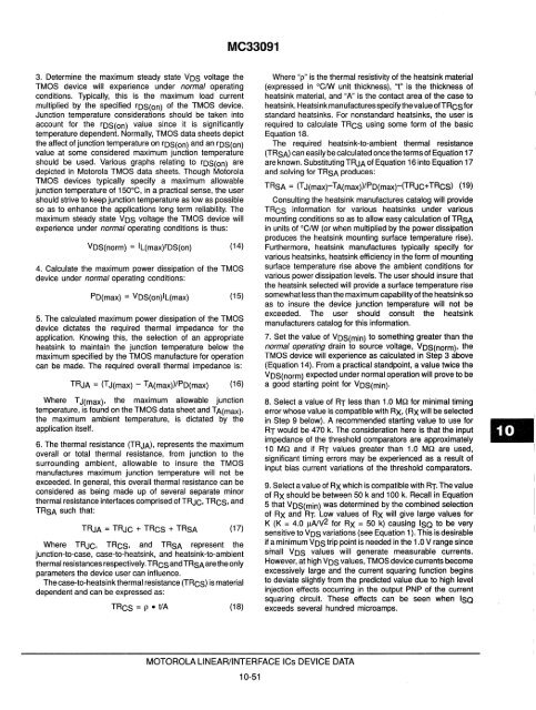
3. Oetermine the maximum steady state VOS voltage the<br />
TMOS device will experience under normal operating<br />
conditions. Typically, this is the maximum load current<br />
multiplied by the specified rOS(on) of the TMOS device.<br />
Junction temperature considerations should be taken into<br />
account for the rOS(on) value since it is significantly<br />
temperature dependent. Normally, TMOS data sheets depict<br />
the affect of junction temperature on rOS(on) and an rOS(on)<br />
value at some considered maximum junction temperature<br />
should be used. Various graphs relating to rOS(on) are<br />
depicted in Motorola TMOS data sheets. Though Motorola<br />
TMOS devices typically specify a maximum allowable<br />
junction temperature of 150°C, in a practical sense, the user<br />
should strive to keep junction temperature as low as possible<br />
so as to enhance the applications long term reliability. The<br />
maximum steady state VOS voltage the TMOS device will<br />
experience under normal operating conditions is thus:<br />
VOS(norm) = IL(max)rOS(on) (14)<br />
4. Calculate the maximum power dissipation of the TMOS<br />
device under normal operating conditions:<br />
PO(max) = VOS(on)IL(max)<br />
MC33091<br />
(15)<br />
5. The calculated maximum power dissipation of the TMOS<br />
device dictates the required thermal impedance for the<br />
application. Knowing this, the selection of an appropriate<br />
heatsink to maintain the junction temperature below the<br />
maximum specified by the TMOS manufacture for operation<br />
can be made. The required overall thermal impedance is:<br />
TRJA = (TJ(max) - TA(max))/PO(max) (16)<br />
Where T J(max), the maximum allowable junction<br />
temperature, is found on the TMOS data sheet and TA(max),<br />
the maximum ambient temperature, is dictated by the<br />
application itself.<br />
6. The thermal resistance (TRJA), represents the maximum<br />
overall or total thermal resistance, from junction to the<br />
surrounding ambient, allowable to insure the TMOS<br />
manufactures maximum junction temperature will not be<br />
exceeded. In general, this overall thermal resistance can be<br />
considered as being made up of several separate minor<br />
thermal resistance interfaces comprised of TRJC, TRCS, and<br />
TRSA such that:<br />
TAJA = TAJC + TACS + TASA (17)<br />
Where TRJC, TRCS, and TRSA represent the<br />
junction-to-case, case-to-heatsink, and heatsink-to-ambient<br />
thermal resistances respectively. TRCS and TRSA are the only<br />
parameters the device user can influence.<br />
The case-to-heatsink thermal resistance (TRCS) is material<br />
dependent and can be expressed as:<br />
TRCS = P • tlA (18)<br />
MOTOROLA LINEAR/INTERFACE ICs DEVICE DATA<br />
10-51<br />
Where "p" is the thermal resistivity of the heatsink material<br />
(expressed in °C/W unit thickness), ''I'' is the thickness of<br />
heats ink material, and "A" is the contact area of the case to<br />
heatsink. Heatsink manufactures specify the value ofTRCS for<br />
standard heatsinks. For nonstandard heatsinks, the user is<br />
required to calculate TRCS using some form of the basic<br />
Equation 18.<br />
The required heatsink-to-ambient thermal resistance<br />
(TRSA) can easily be calculated once the terms of Equation 17<br />
are known. Substituting TRJA of Equation 16 into Equation 17<br />
and solving for TRSA produces:<br />
TRSA = (TJ(max)-TA(max))/PO(maxHTRJC+TRCS) (19)<br />
Consulting the heatsink manufactures catalog will provide<br />
TRCS information for various heatsinks under various<br />
mounting conditions so as to allow easy calculation of TRSA<br />
in units of °C/W (or when multiplied by the power dissipation<br />
produces the heatsink mounting surface temperature rise).<br />
Furthermore, heatsink manufactures typically specify for<br />
various heatsinks, heatsink efficiency in the form of mounting<br />
surface temperature rise above the ambient conditions for<br />
various power dissipation levels. The user should insure that<br />
the heatsink selected will provide a surface temperature rise<br />
somewhat less than the maximum capability ofthe heatsink so<br />
as to insure the device junction temperature will not be<br />
exceeded. The user should consult the heatsink<br />
manufacturers catalog for this information.<br />
7. Set the value of VOS(min) to something greater than the<br />
normal operating drain to source voltage, VOS(norm), the<br />
TMOS device will experience as calculated in Step 3 above<br />
(Equation 14). From a practical standpoint, a value twice the<br />
VOS(norm) expected under normal operation will prove to be<br />
a good starting point for VOS(min)'<br />
8. Select a value of RT less than 1.0 Mil for minimal timing<br />
error whose value is compatible with RX, (RX will be selected<br />
in Step 9 below). A recommended starting value to use for<br />
RT would be 470 k. The consideration here is that the input<br />
impedance of the threshold comparators are approximately<br />
10 Mil and if RT values greater than 1.0 Mil are used,<br />
significant timing errors may be experienced as a result of<br />
input bias current variations of the threshold comparators.<br />
9. Select a value of RX which is compatible with RT. The value<br />
of RX should be between 50 k and 100 k. Recall in Equation<br />
5 that VOS(min) was determined by the combined selection<br />
of RX and RT. Low values of RX will give large values for<br />
K (K = 4.0 IJAIV2 for RX = 50 k) causing Isa to be very<br />
sensitive to VOS variations (see Equation 1). This is desirable<br />
if a minimum VOS trip point is needed in the 1.0 V range since<br />
small VOS values will generate measurable currents.<br />
However, at high VOS values, TMOS device currents become<br />
excessively large and the current squaring function begins<br />
to deviate slightly from the predicted value due to high level<br />
injection effects occurring in the output PNP of the current<br />
squaring circuit. These effects can be seen when Isa<br />
exceeds several hundred microamps.<br />
,<br />
IIII


