Voltage References
Voltage References
Voltage References

You also want an ePaper? Increase the reach of your titles
YUMPU automatically turns print PDFs into web optimized ePapers that Google loves.
Darlington Drive<br />
The Darlington Drive output pin exists to turn on a power<br />
Darlington. The Sense pin voltage determines the duty<br />
cycle of the Darlington. The oscillator is set to maintain a<br />
minimum duty cycle, except during overvoltage and short<br />
circuit conditions.<br />
Short Circuit<br />
The Short Circuit pin monitors the field voltage. When the<br />
Darlington Drive and Short Circuit pins are simultaneously<br />
high for a duration greater than the slew rate period, a short<br />
circuit condition is noted. The detection time required prevents<br />
the device from reacting to false shorts. As a result of short<br />
Introduction<br />
Although the packaging technology known as "flip-chip" has<br />
been available for some time, it has seen few applications<br />
outside the automotive and computer industries. Present<br />
microelectronic trends are demanding smaller chip sizes,<br />
reduced manufacturing costs, and improved reliability.<br />
Flip-chip technology satisfies all of these needs.<br />
Conventional assembly techniques involve bonding wires<br />
to metal pads to make electrical contact to the integrated<br />
circuit. Flip-chip assembly requires further processing of the<br />
integrated circuit after final nitride deposition to establish<br />
robust solder bumps with which to make electrical contact to<br />
the circuit. Aspatially identical solderable solder bump pattern,<br />
normally formed on ceramic material, serves as a substrate<br />
host for the flip-chip. The "bumped" flip-chip is aligned to, and<br />
temporally held in place through the use of soldering paste.<br />
The aligned flip-chip and substrate host are placed into an<br />
oven and the solder reflowed to establish both electrical and<br />
mechanical bonding of the flip-chip to the substrate circuit.<br />
Use of solder paste not only holds the chip in temporary<br />
placement for reflow but also enhances the reflow process to<br />
produce highly reliable bonds.<br />
Flip-Chip Benefits<br />
Some of the benefits of flip-chip assembly are:<br />
1) Higher circuit density resulting in approximately<br />
one-tenth the footprint required of a conventional<br />
plastic encapsulated device.<br />
2) Improved reliability especially in high temperature<br />
applications. This is due, in part, to the absence<br />
of wires to corrode or fatigue from extensive<br />
thermal cycling.<br />
3) No bond wires are required that might possibly<br />
become damaged during assembly.<br />
4) Adaptable for simultaneous assembly of multiple<br />
flip-chips, in a hybrid fashion, onto a single<br />
ceramic substrate.<br />
The following discussion covers the flip-chip process steps<br />
performed by Motorola, and the assembly processing<br />
required by the customer, in order to attach the flip-chip onto<br />
a ceramic substrate.<br />
MOTOROLA'S FLIP-CHIP PROCESS<br />
Overview<br />
The process steps to develop an integrated circuit flip-chip<br />
are identical to that of conventional integrated circuits up to<br />
MCCF33095<br />
FLIP-CHIP APPLICATION INFORMATION<br />
MOTOROLA LINEAR/INTERFACE ICs DEVICE DATA<br />
10-69<br />
circuit detection, the output is disabled. During a short circuit<br />
condition the device automatically retries with a 2% duty cycle<br />
(Darlington ON). Once the short circuit condition ceases,<br />
normal device operation resumes.<br />
Note<br />
A capacitor should be used in parallel with the VCC pin<br />
to filter out noise transients. Likewise, a capacitor should be<br />
used in parallel with the Sense pin to create a dominant<br />
closed-loop pole. Resistors connected to inputs, as<br />
mentioned in Notes 1 through 5 of the Electrical Characteristic<br />
table, should be used.<br />
and including the deposition of the final nitride paSSivation<br />
layer on the front surface (circuit side). At this stage all device<br />
metal interconnects are present.<br />
The process sequence is as follows:<br />
1) Passivation-nitride photo resist and etch<br />
2) Bimetal sputter (titanium (Ti) and tungsten (W)<br />
followed by copper (Cu))<br />
3) Photo mask to define the bump area<br />
4) Copper plate<br />
5) Lead plate<br />
6) Tin plate<br />
7) Photoresist clean to remove all photo resist material<br />
8) Bimetal etchback<br />
9) Reflow for bump formation<br />
10) Final inspection<br />
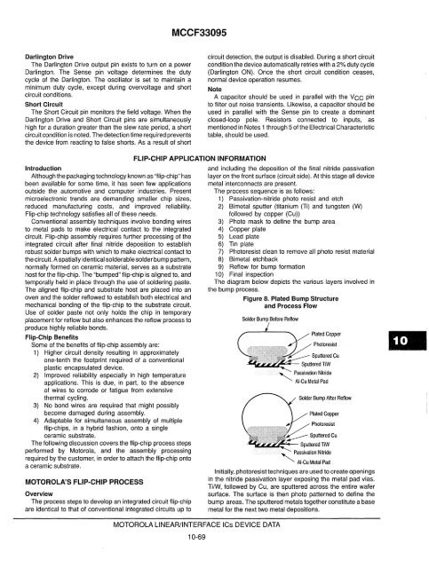
The diagram below depicts the various layers involved in<br />
the bump process.<br />
Figure 8. Plated Bump Structure<br />
and Process Flow<br />
Solder Bump After Reflow<br />
Plated Copper<br />
Initially, photoresist techniques are used to create openings<br />
in the nitride passivation layer exposing the metal pad vias.<br />
TilW, followed by Cu, are sputtered across the entire wafer<br />
surface. The surface is then photo patterned to define the<br />
bump areas. The sputtered metals together constitute a base<br />
metal for the next two metal depositions.