Voltage References
Voltage References
Voltage References

You also want an ePaper? Increase the reach of your titles
YUMPU automatically turns print PDFs into web optimized ePapers that Google loves.
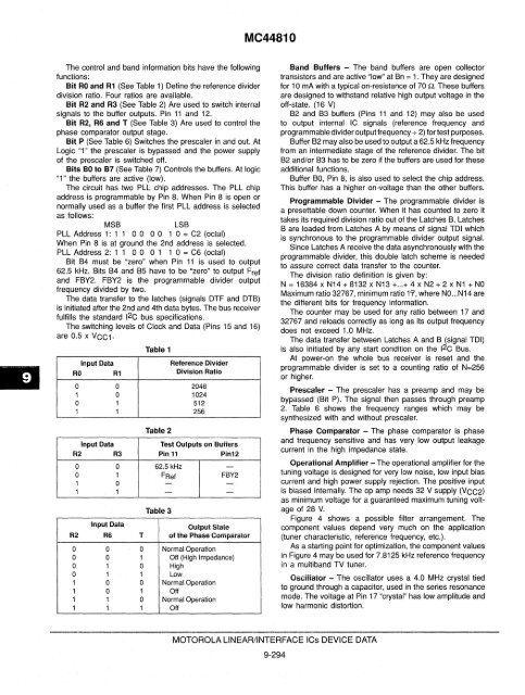
The control and band information bits have the following<br />
functions:<br />
Bit RO and R1 (See Table 1) Define the reference divider<br />
division ratio. Four ratios are available.<br />
Bit R2 and R3 (See Table 2) Are used to switch internal<br />
signals to the buffer outputs. Pin 11 and 12.<br />
Bit R2, R6 and T (See Table 3) Are used to control the<br />
phase comparator output stage.<br />
Bit P (See Table 6) Switches the prescaler in and out. At<br />
Logic "1' the prescaler is bypassed and the power supply<br />
of the prescaler is switched off.<br />
Bits BO to B7 (See Table 7) Controls the buffers. At logic<br />
"1" the buffers are active (low).<br />
The circuit has two PLL chip addresses. The PLL chip<br />
address is programmable by Pin 8. When Pin 8 is open or<br />
normally used as a buffer the first PLL address is selected<br />
as follows:<br />
MSB LSB<br />
PLL Address 1: 1 1 a a a a 1 0= C2 (octal)<br />
When Pin 8 is at ground the 2nd address is selected.<br />
PLL Address 2: 1 1 a a a 1 1 a = C6 (octal)<br />
Bit B4 must be "zero" when Pin 11 is used to output<br />
62.5 kHz. Bits B4 and B5 have to be "zero" to output Fref<br />
and FBY2. FBY2 is the programmable divider output<br />
frequency divided by two.<br />
The data transfer to the latches (signals OTF and OTB)<br />
is initiated after the 2nd and 4th data bytes. The bus receiver<br />
fulfills the standard 12C bus specifications.<br />
The switching levels of Clock and Data (Pins 15 and 16)<br />
are 0.5 x VCC1.<br />
Table 1<br />
Input Data Reference Divider<br />
RO R1 Division Ratio<br />
0 0 2048<br />
1 0 1024<br />
0 1 512<br />
1 1 256<br />
Table 2<br />
Input Data Test Outputs on Buffers<br />
R2 R3 Pin 11 Pln12<br />
0 0 62.5 kHz -<br />
0 1 FRet FBY2<br />
1 0 - -<br />
1 1 - -<br />
Table 3<br />
Input Data Output Slate<br />
R2 R6 T of the Phase Comparator<br />
0 0 0 Normal Operation<br />
0 0 1 Off (High Impedance)<br />
0 1 0 High<br />
0 1 1 Low<br />
1 0 0 Normal Operation<br />
1 0 1 Off<br />
1 1 0 Normal Operation<br />
1 1 1 Off<br />
MC44810<br />
MOTOROLA LINEAR/INTERFACE ICs DEVICE DATA<br />
9-294<br />
Band Buffers - The band buffers are open collector<br />
transistors and are active "low" at Bn = 1. They are designed<br />
for 10 mA with a typical on-resistance of 70 Q. These buffers<br />
are designed to withstand relative high output voltage in the<br />
off-state. (16 V)<br />
B2 and B3 buffers (Pins 11 and 12) may also be used<br />
to output internal IC signals (reference frequency and<br />
programmable divider output frequency + 2) for test purposes.<br />
Buffer B2 may also be used to output a 62.5 kHz frequency<br />
from an intermediate stage of the reference divider. The bit<br />
B2 and/or B3 has to be zero if the buffers are used for these<br />
additional functions.<br />
Buffer BO, Pin 8, is also used to select the chip address.<br />
This buffer has a higher on-voltage than the other buffers.<br />
Programmable Divider - The programmable divider is<br />
a presettable down counter. When it has counted to zero it<br />
takes its required division ratio out of the Latches B. Latches<br />
B are loaded from Latches A by means of signal TDI which<br />
is synchronous to the programmable divider output signal.<br />
Since Latches A receive the data asynchronously with the<br />
programmable divider, this double latch scheme is needed<br />
to assure correct data transfer to the counter.<br />
The division ratio definition is given by:<br />
N = 16384 x N14+8132 x N13 + ... + 4 x N2+2 x N1 + NO<br />
Maximum ratio 32767, minimum ratio 1'7, where NO ... N14 are<br />
the different bits for frequency information.<br />
The counter may be used for any ratio between 17 and<br />
32767 and reloads correctly as long as its output frequency<br />
does not exceed 1.0 MHz.<br />
The data transfer between Latches A and B (signal TOI)<br />
is also initiated by any start condition on the 12C Bus.<br />
At power-on the whole bus receiver is reset and the<br />
programmable divider is set to a counting ratio of N=256<br />
or higher.<br />
Prescaler - The prescaler has a preamp and may be<br />
bypassed (Bit Pl. The signal then passes through preamp<br />
2. Table 6 shows the frequency ranges which may be<br />
synthesized with and without prescaler.<br />
Phase Comparator - The phase comparator is phase<br />
and frequency sensitive and has very low output leakage<br />
current in the high impedance state.<br />
Operational Amplifier - The operational amplifier for the<br />
tuning voltage is designed for very low nOise, low input bias<br />
current and high power supply rejection. The positive input<br />
is biased internally. The op amp needs 32 V supply (VCC2)<br />
as minimum voltage for a guaranteed maximum tuning voltage<br />
of 28 V.<br />
Figure 4 shows a possible filter arrangement. The<br />
component values depend very much on the application<br />
(tuner characteristic, reference frequency, etc.).<br />
As a starting point for optimization, the component values<br />
in Figure 4 may be used for 7.8125 kHz reference frequency<br />
in a multiband TV tuner.<br />
Oscillator - The oscillator uses a 4.0 MHz crystal tied<br />
to ground through a capacitor, used in the series resonance<br />
mode. The voltage at Pin 17 "crystal" has low amplitude and<br />
low harmonic distortion.