Voltage References
Voltage References
Voltage References

Create successful ePaper yourself
Turn your PDF publications into a flip-book with our unique Google optimized e-Paper software.
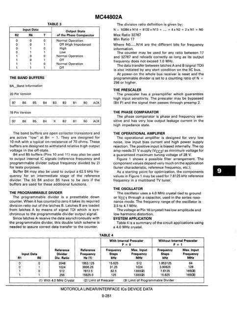
TABLE 3<br />
Input Data<br />
Output State<br />
R2 R6 T of the Phase Compamtor<br />
0 0 0 Normal Operation<br />
0 0 1 Off (High Impedance)<br />
0 1 0 High<br />
0 1 1 Low<br />
1 0 0 Normal Operation<br />
1 0 1 Off<br />
1 1 0 Normal Operation<br />
1 1 1 Off<br />
THE BAND BUFFERS<br />
BA_ Band Information<br />
20 Pin Version<br />
I B7 B6 B5 B4 B3 B2 B1 BO ACKi<br />
18 Pin Version<br />
EB6 B5 B4 X B2 B1 BO ACKi<br />
The band buffers are open collector transistors and<br />
are active "low" at Bn = 1. They are designed for<br />
10 mA with a typical on-resistance of 70 ohms. These<br />
buffers are designed to withstand relative high output<br />
voltage in the off-state.<br />
B4 and B5 buffers (Pins 10 and 11) may also be used<br />
to output internal IC signals (reference frequency and<br />
programmable divider output frequency divided by 2)<br />
for tests purposes.<br />
Buffer B4 may also be used to output a 62.5 kHz frequency<br />
for an intermediate stage of the reference<br />
divider. The bit B4 andlor B5 have to be zero if the<br />
buffers are used for these additional functions.<br />
THE PROGRAMMABLE DIVIDER<br />
The programmable divider is a presettable down<br />
counter. When it has counted to zero it takes its required<br />
division ratio out of the latches B. Latches B are loaded<br />
from latches A by means of signal TDI which is synchronous<br />
to the programmable divider output signal.<br />
Since latches A receive the data asynchronously with<br />
the programmable divider, this double latch scheme is<br />
needed to assure correct data transfer to the counter.<br />
Input Data<br />
R1<br />
0<br />
0<br />
1<br />
1<br />
MC44802A<br />
TABLE 4<br />
The division ratio definition is given by:<br />
N = 16384xN14 + 8132xN13 + ..... + 4xN2 + 2xN1 + NO<br />
Max Ratio 32767<br />
Min Ratio 17<br />
Where NO ....... N14 are the different bits for frequency<br />
information.<br />
The counter may be used for any ratio between 17<br />
and 32767 and reloads correctly as long as its output<br />
frequency does not exceed 1.0 MHz.<br />
The data transfer between latches A and B (signal TDI)<br />
is also initiated by any start condition on the IIC bus.<br />
At power-on the whole bus receiver is reset and the<br />
programmable divider is set to a counting ratio of N<br />
256 or higher.<br />
THE PRESCALER<br />
The prescaler has a preamplifier which guarantees<br />
high input sensitivity. The prescaler may be bypassed<br />
(Bit P) and the signal then passes through preamp 2.<br />
THE PHASE COMPARATOR<br />
The phase comparator is phase and frequency sensitive<br />
and has very low output leakage current in the<br />
high impedance state.<br />
THE OPERATIONAL AMPLIFIER<br />
The operational amplifier is designed for very low<br />
noise, low input bias current and high power supply<br />
rejection. The positive input is biased internally. The op<br />
amp needs 31 V supply (VCC2) as minimum voltage for<br />
a guaranteed maximum tuning voltage of 28 V.<br />
Figure 1 shows a possible filter arrangement. The<br />
component values depend very much on the application<br />
(tuner characteristic, reference frequency, etc.);<br />
As a starting point for optimization, the components<br />
values in Figure 1 may be used for 7.8125 kHz reference<br />
frequency in a multi band TV tuner.<br />
THE OSCILLATOR<br />
The oscillator uses a 4.0 MHz crystal tied to ground<br />
or VCC1 through a capacitor, used in the series resonance<br />
mode. The frequency range of the oscillator is<br />
3.5 to 4.1 MHz.<br />
Thevoltage at Pin 16 (crystal) has low amplitude and<br />
low harmonic distortion.<br />
SYSTEM APPLICATION<br />
Table 4 is a summary of the circuit applications using<br />
a 4.0 MHz crystal.<br />
With Internal Prescaler Without Internal Prescaler<br />
P = 0 P = 1<br />
Reference Reference Frequency Max. Input Frequency Max. Input<br />
Divider Frequency Steps Frequency Steps Frequency<br />
RO Div. Ratio Hz (1) kHz MHz kHz MHz<br />
0 2048 1953.125 15.625 512 1.953125 64<br />
1 1024 3906.25 31.25 1024 3.90625 128<br />
0 512 7812.5 62.5 1300(2) 7.8125 165(3)<br />
1 256 15625.0 125 1300(2) 15.625 165(3)<br />
(1) With 4.0 MHz Crystal (2) Limit of Prescaler (3) Limit of Programmable Divider<br />
MOTOROLA LINEAR/INTERFACE ICs DEVICE DATA<br />
9-281