Voltage References
Voltage References
Voltage References

Create successful ePaper yourself
Turn your PDF publications into a flip-book with our unique Google optimized e-Paper software.
The MC1330A offers the designer a new approach to an old<br />
problem. Now linear detection can be performed at much<br />
lower power Signal levels than possible with a detector diode.<br />
Offering a number of distinct advantages, its easy implementation<br />
should meet with ready acceptance for television<br />
designs. Some specific features and information on systems<br />
design with this device are given below:<br />
1. The device provides excellent linearity of output versus<br />
input, as shown in Figures 6 and 7. These graphs also<br />
show that video peak-to-peak amplitude (AC) does not<br />
change with supply voltage variation. (Slopes are parallel.<br />
Visualize a given variation of input CW and use the figure as<br />
a transfer function.)<br />
2. The DC output level does change linearly with supply<br />
voltage shown if Figure 8. This can be accommodated by<br />
regulating the supply or by referencing the subsequent video<br />
amplifier to the same power supply.<br />
3. The choice of a for the tuned circuit of Pin 2 and 3 is not<br />
critical. The higher the a, the better the rejection of 920 kHz<br />
products by the more critical the tuning accuracy required (see<br />
A very compact high performance IF amplifier constructed<br />
as shown in Figure 14 minimizes the number of overall<br />
components and alignment adjustments. It can be readily<br />
combined with normal tuners and input tuning-trapping<br />
circuitry to provide the performance demanded of high quality<br />
receivers. This configuration will provide approximately 93 dB<br />
voltage gain and can accommodate the usual low impedance<br />
input network or, if desired, can take advantage of an<br />
impedance step-up from tuner to MC1350 input.<br />
The burden of selectivity, formerly found between the third<br />
IF and detector, must now be placed at the interstage.<br />
The nominal 3.0 V peak-to-peak output can be varied from 0<br />
V to 7.0 V with excellent linearity and freedom from spurious<br />
output products.<br />
Alignment is most easily accomplished with an AM generator,<br />
set at a carrier frequency of 45.75 MHz, modulated with a<br />
video frequency sweep. This provides the proper realistic<br />
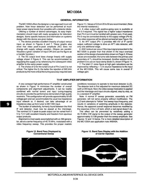
Figure 12. Band Pass Displayed by<br />
Conventional Sweep<br />
MC1330A<br />
GENERAL INFORMATION<br />
TV·IF AMPLIFIER INFORMATION<br />
MOTOROLA LINEAR/INTERFACE ICs DEVICE DATA<br />
9-34<br />
Figure 11). Values of a from 20 to 50 are recommended. (Note<br />
the internal reSistance.)<br />
4. A video output with positive-going sync is available at<br />
Pin 5 if required. This signal has a higher output impedance<br />
than Pin 4 so it must be handled with greater care. If not used,<br />
Pin 5 may be connected directly to the supply voltage (Pin 6).<br />
The video response will be altered somewhat (see Figure 10).<br />
5. An AFT output (Pin 1) provides 460 mV of IF carrier<br />
output, sufficient voltage to drive an AFT ratio detector, with<br />
only one additional stage.<br />
6. AGC lockout can occur if the input signal presented in the<br />
MC1330A is greater than that shown in the input overload<br />
section of the design characteristics shown on Page 3. If these<br />
values are exceeded, the turns ratio between the primary and<br />
secondary of T 1 should be increased. Another solution to the<br />
problem is to use an input clamp diode D1 shown if Figure 14.<br />
7. The totall.F. noise figure at high gain reductions can be<br />
improved by reflecting = 1.0 k source impedance to the input<br />
of the MC1330A. This will cause some loss in overall IF<br />
voltage gain.<br />
conditions necessary to operate to lOW-level detector (LLD).<br />
The detector tank is first adjusted for maximum detected DC<br />
(with a CW input). Next, the video sweep modulation is applied<br />
and the interstage and input circuits aligned, step by step, as<br />
in a standard IF amplifier.<br />
Note: A normal IF sweep generator, essentially an FM<br />
generator, will not serve properly without modification. The<br />
LLD tank attempts to "follow" the sweep input frequency, and<br />
results in variations of switching amplitude in the detector.<br />
Hence, the apparent overall response becomes modified by<br />
the response of the LLD tank, which a real signal doesn't do.<br />
This effect can be prevented by reSistively adding a<br />
45.75 MHz CW signal to the output of the sweep generator<br />
approximately 3.0 dB greater than the sweep amplitude. See<br />
Figures 12 and 13 below. For a more detailed description of<br />
the MC1330A see application note AN545A.<br />
Figure 13. Band Pass Display with the Addition<br />
of Carrier Injection