Voltage References
Voltage References
Voltage References
You also want an ePaper? Increase the reach of your titles
YUMPU automatically turns print PDFs into web optimized ePapers that Google loves.
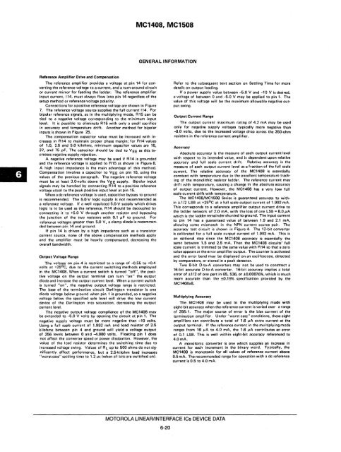
Reference Amplifier Drive and Compensation<br />
The reference amplifier provides a voltage at pin 14 for converting<br />
the reference voltage to a current, and a turn-around circuit<br />
or current mirror for feeding the ladder. The reference amplifier<br />
input current, 114. must always flow into pin 14 regardless of the<br />
setup method or reference voltage polarity.<br />
Connections for a positive reference voltage arB shown in Figure<br />
7. The reference voltage source supplies the full current 114. For<br />
bipolar reference signals. as in the multiplying mode, R15 can be<br />
tied to a negative voltage corresponding to the minimum input<br />
level. It is possible to eliminate R15 with only a small sacrifice<br />
in accuracy and temperature drift. Another method for bipolar<br />
inputs is shown in Figure 25.<br />
The compensation capacitor value must be increased with increases<br />
in R14 to maintain proper phase margin; for R14 values<br />
of 1.0, 2.5 and 5.0 kilohms, minimum capacitor values are 15,<br />
37, and 75 pF. The capacitor "should be"tied to VEE as this increases<br />
negative supply rejection.<br />
A negative reference voltage may be used if R14 is grounded<br />
and the reference voltage is applied to R15 as shown in Figure 8.<br />
A high input impedance is the main advantage of this method.<br />
Compensation involves a capacitor to VEE on pin 16, using the<br />
values of the previous paragraph. The negative reference voltage<br />
must be at least 3.0-volts above the VEE supply. Bipolar input<br />
signals may be handled by connecting R 14 to a positive reference<br />
voltage equal to the peak positive input level at pin 15.<br />
When a dc reference voltage is used, capacitive bypass to ground<br />
is recommended. The 5.O-V logic supply is not recommended as<br />
a reference voltage. If a well regulated 5.O-V supply which drives<br />
logic is to be used as the reference, R14 should be decoupled by<br />
connecting it to +5.0 V through another resistor and bypassing<br />
the junction of the two resistors with 0.1 #'F to ground. For<br />
reference voltages greater than 5.0 V, a clamp diode is recommended<br />
betvveen pin 14 and ground.<br />
If pin 14 is driven by a high impedance such as a transistor<br />
current source, none of the above compensation methods apply<br />
and the amplifier must be heavily compensated, decreasing the<br />
overall bandwidth.<br />
Output <strong>Voltage</strong> Range<br />
The voltaae on pin 4 is restricted to a range of -0.55 to +0.4<br />
volts at +25 C, due to the current switching methods employed<br />
in the MC1408. When a current switch Is turned "off". the positive<br />
voltage on the output terminal can turn "on" the output<br />
diode and increase the output current level. When a current switch<br />
is turned "on", the negative output voltage range is restricted.<br />
The base of the termination circuit Darlington transistor is one<br />
diode voltage below ground when pin 1 is grounded, so a negative<br />
voltage below the specified safe level will drive the low current<br />
device of the Darlington into saturation, decreasing the output<br />
current level.<br />
The negative output voltage compliance of the MC140B may<br />
be extended to -5.0 V volts by opening the circuit at pin 1. The<br />
negative supply voltage must be more negative than -10 volts.<br />
Using a full scale current of 1.992 mA and" load resistor of 2.5<br />
kilohms betvveen pin 4 and ground will yield a voltage output<br />
of 256 levels between 0 and -4.9S0 volts. Floating pin 1 does<br />
not affect the converter speed or power dissipation. However, the<br />
value of the load resistor determines the switching time due to<br />
increased voltage swing. Values of RL up to 500 ohms do not significantly<br />
affect performance, but a 2.5-kilohm load increases<br />
"worst case" settling time to 1.2#'s (when all bits are switched on).<br />
MC1408, MC1508<br />
GENERAL INFORMATION<br />
Refer to the subsequent text section on Settling Time for more<br />
details on output loading.<br />
If a power supply value between -5.0 V and -10 V is desired,<br />
a voltage of between 0 and -5.0 V may be applied to pin 1. The<br />
value of this voltage will be the maximum allowable negative output<br />
swing.<br />
Output Current Range<br />
The output current maximum rating of 4.2 rnA may be used<br />
only for negative supply voltages typically more negative than<br />
-B.O volts, due to the increased voltage drop across the 350-ohm<br />
resistors in the reference current amplifier.<br />
Accuracy<br />
Absolute accuracy is the measure of each output current level<br />
with respect to its intended value, and is dependent upon relative<br />
accuracy and full scale current drift. Relative accuracy is the<br />
measure of each output current level as a fraction of the full scale<br />
current. The relative accuracy of the MC1408 is essentially<br />
constant with temperature due to the excellent temperature track·<br />
ing of the monolithic resistor ladder. The reference current may<br />
drift with temperature, causing a change in the absolute accuracy<br />
of output current. However, the MC1408 has a very low full<br />
scale current drift with temperature.<br />
The MC140S/MC150S Series is guaranteed accurate to within<br />
± 1/2 LSB at +250 C at a full scale output current of 1.992 rnA.<br />
This corresponds to a reference amplifier output current drive to<br />
the ladder network of 2.0 rnA, with the loss of one LSB = S.O jlA<br />
which is the ladder remainder shunted to ground. The input current<br />
to pin 14 has a guaranteed value of between 1.9 and 2.1 rnA,<br />
allowing some mismatch in the NPN current source pair. The<br />
accuracy test circuit is shown in Figure 4. The 12-bit converter<br />
is calibrated for a full scale output current of 1.992 mAo This is<br />
an optional step since the MC1408 accuracy is essentially the<br />
same between 1.5 and 2.5 rnA. Than the MC140S ·circuits' full<br />
scale current is trimmed to the same value with R 14 so that a zero<br />
value appears at the error ampl ifier output. The counter is activated<br />
and the error band may be displayed on an oscilloscope, detected<br />
by comparators, or stored in a peak detector.<br />
Two 8-bit D-to-A converters may not be used to construct a<br />
16-bit accurate D-to-A converter. 16-bit accuracy implies a total<br />
error of ±1/2 of one part in 65, 536, or ±0.OOO76%, which is much<br />
more accurate than the ±'o.19% specification provided bV the<br />
MCI408xS.<br />
Multiplying Accuracy<br />
MOTOROLA LINEAR/INTERFACE ICs DEVICE DATA<br />
6-20<br />
The MC1408 may be used in the multiplying mode with<br />
eight-bit accuracy when the reference current is varied over a range<br />
of 256:1. The major source of error is the bias current of the<br />
termination amplifier. Under "worst case" conditions, these eight<br />
amplifiers can contribute a total of 1.6 #'A extra current at the<br />
output terminal. If the reference current in the multiplying mode<br />
ranges from 16 SLA to 4.0 mA, the 1.6 IlA contributes an error<br />
of 0.1 LS8. This is well within eight-bit accuracy referenced to<br />
4.0mA.<br />
A monotonic converter is one which supplies an increase in<br />
current for each increment in the binary word. Typically, the<br />
MC1408 is monotonic for all values of reference current above<br />
0.5 mAo The recommended range for operation with a dc reference<br />
current is 0.5 to 4.0 mAo


