Voltage References
Voltage References
Voltage References

You also want an ePaper? Increase the reach of your titles
YUMPU automatically turns print PDFs into web optimized ePapers that Google loves.
Composite Sync Separator<br />
The composite sync separation section comprises two<br />
blocks, a sync slicer and a sync amplifier, that can be used to<br />
extract the vertical sync information from a video signal.<br />
The sync separator is an adaptive slicer in which the video<br />
signal is slightly integrated and then sliced at a ratio of 4.7 to<br />
64 which corresponds to the sync to horizontal ratio. Two<br />
outputs are given, one of high impedance and the other low<br />
impedance.<br />
A slicing sync inverting amplifier is also on-chip, allowing<br />
one output to be used for composite sync and the other<br />
output to be integrated and then sliced using the slicing<br />
amplifier to extract the vertical sync information.<br />
Clock Generation<br />
The clock generation is made up of a wide ranging<br />
emitter-coupled VCO followed by a switchable .,. 2 to provide<br />
a 50% duty cycle wherever required, or twice the set<br />
frequency if an external divider is used. The clock generation<br />
is a PLL subsection. Its function is the generation of a high<br />
frequency, line-locked clock that is used for video sampling<br />
and digitizing.<br />
MC44145<br />
CIRCUIT DESCRIPTION<br />
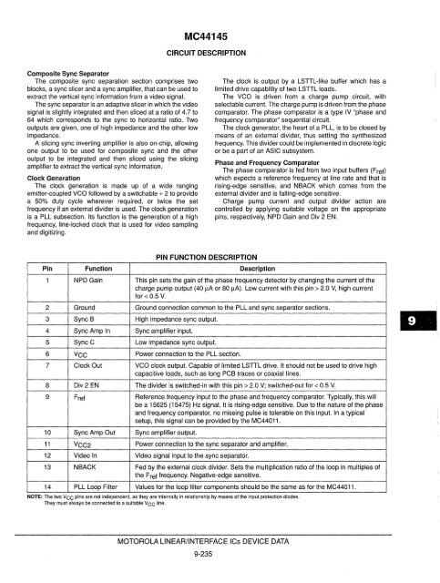
PIN FUNCTION DESCRIPTION<br />
Pin Function Description<br />
The clock is output by a LSTTL-like buffer which has a<br />
limited drive capability of two LSTTL loads.<br />
The VCO is driven from a charge pump circuit, with<br />
selectable current. The charge pump is driven from the phase<br />
comparator. The phase comparator is a type IV "phase and<br />
frequency comparator" sequential circuit.<br />
The clock generator, the heart of a PLL, is to be closed by<br />
means of an external divider, thus setting the synthesized<br />
frequency. This divider could be implemented in discrete logic<br />
or be a part of an ASIC subsystem.<br />
Phase and Frequency Comparator<br />
The phase comparator is fed from two input buffers (Fref)<br />
which expects a reference frequency at line rate and that is<br />
rising-edge sensitive, and NBACK which comes from the<br />
external divider and is falling-edge sensitive.<br />
Charge pump current and output divider action are<br />
controlled by applying suitable voltage on the appropriate<br />
pins, respectively, NPD Gain and Div 2 EN.<br />
1 NPD Gain This pin sets the gain of the phase frequency detector by changing the current of the<br />
charge pump output (40 /.LA or 80 /.LA). Low current with this pin> 2.0 V, high current<br />
for < 0.5 V.<br />
2 Ground Ground connection common to the PLL and sync separator sections.<br />
3 Sync B High impedance sync output.<br />
4 Sync Amp In Sync amplifier input.<br />
5 SyncC Low impedance sync output.<br />
6 VCC Power connection to the PLL section.<br />
7 Clock Out VCO clock output. Capable of limited LSTTL drive. It should not be used to drive high<br />
capacitive loads, such as long PCB traces or coaxial lines.<br />
8 Div 2 EN The divider is switched-in with this pin> 2.0 V; switched-out for < 0.5 V.<br />
9 Fref Reference frequency input to the phase and frequency comparator. Typically, this will<br />
be a 15625 (15475) Hz signal. It is rising-edge sensitive. Due to the nature of the phase<br />
and frequency comparator, no missing pulse is tolerable on this input. In a typical<br />
setup, this signal can be provided by the MC44011.<br />
10 Sync Amp Out Sync amplifier output.<br />
11 VCC2 Power connection to the sync separator and amplifier.<br />
12 Video In Video signal input to the sync separator.<br />
13 NBACK Fed by the external clock divider. Sets the multiplication ratio of the loop in multiples of<br />
the Fref frequency. Negative-edge sensitive.<br />
14 PLL Loop Filter Values for the loop filter components should be the same as for the MC44011.<br />
NOTE: The two vee pins are not independent. as they are internally in relationship by means of the input protection diodes.<br />
They must always be connected to a suitable Vee line.<br />
MOTOROLA LINEAR/INTERFACE ICs DEVICE DATA<br />
9-235