Voltage References
Voltage References
Voltage References

Create successful ePaper yourself
Turn your PDF publications into a flip-book with our unique Google optimized e-Paper software.
applied to the reference must be such that the absolute<br />
voltage at VRT and VRB are maintained within the values<br />
listed in the Recommended Operating Limits. The<br />
RMS value of the span must be maintained ,;;;2.1 volts.<br />
POWER SUPPLIES<br />
VCC(A) (Pin 9) is the positive power supply for the<br />
comparators, and VCC(D) (Pins 10, 16) is the positive<br />
power supply forthe digital portion. Both are to be + 5.0<br />
volts, ± 10%, and the two are to be within 100 millivolts<br />
of each other. There is indirect internal coupling<br />
between VCC(D) and VCC(A). If they are powered separately,<br />
and one supply fails, there will be current flow<br />
through the MC10321 to the failed supply.<br />
ICC(A) is nominally 13 mA, and does not vary with<br />
clock frequency or with Vin' but does vary slightly with<br />
VCC(A). ICC(D) is nominally 60 mA, and is independent<br />
of clock frequency. It does vary, however, by 4-5 mA<br />
as Vin is varied from VRT to VRB, and varies directly<br />
with VCC(D).<br />
VEE is the negative power supply forthe comparators,<br />
and is to be within the range - 3.0 to - 6.0 volts. Additionally,<br />
VEE must be at least 1.3 volts more negative<br />
than VRB. lEE is a nominal - 13 mA, and is independent<br />
of clock frequency, Vin and VEE.<br />
For proper operation, the supplies must be bypassed<br />
at the IC. A 10 /LF tantalum, in parallel with a 0.1 /LF<br />
ceramic is recommended for each supply to ground.<br />
DIGITAL SECTION<br />
CLOCK<br />
The Clock input (Pin 15) is TTL compatible with a<br />
typical frequency range of 0 to 30 MHz. There is no duty<br />
cycle limitation, but the minimum low and high times<br />
must be adhered to. See Figure 6 for the input current<br />
requirements.<br />
The conversion sequence is shown in Figure 13, and<br />
is as follows:<br />
- On the rising edge, the data output latches are<br />
latched with old data, and the comparator output<br />
latches are released to follow the input signal (Vin).<br />
- During the high time, the comparators track the<br />
input signal. The data output latches retain the old data.<br />
- On the falling edge, the comparator outputs are<br />
latched with the data immediately prior to this edge.<br />
The conversion to digital occurs within the device, and<br />
the data output latches are released to indicate the new<br />
data in =22 ns.<br />
- During the clock low time, the comparator outputs<br />
remain latched, and the data output latches remain<br />
transparent.<br />
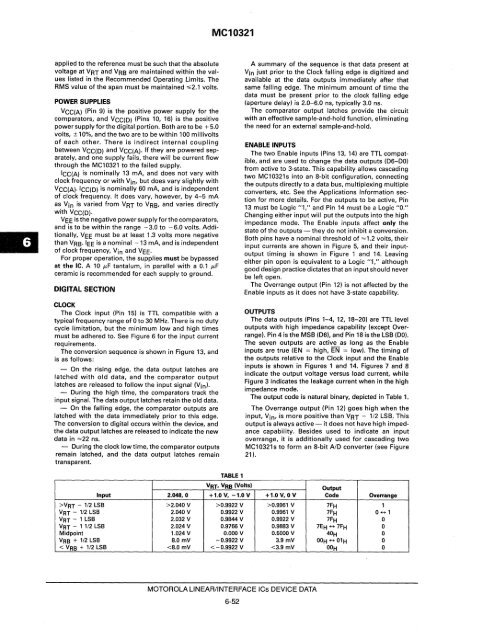
Input<br />
>VRT - 1/2 LSB<br />
VRT - 1/2 LSB<br />
VRT - 1 LSB<br />
VRT - 1 1/2 LSB<br />
Midpoint<br />
VRB + 1/2 LSB<br />
< VRB + 1/2 LSB<br />
MC10321<br />
TABLE I<br />
A summary of the sequence is that data present at<br />
Vin just prior to the Clock falling edge is digitized and<br />
available at the data outputs immediately after that<br />
same falling edge. The minimum amount of time the<br />
data must be present prior to the clock falling edge<br />
(aperture delay) is 2.0-6.0 ns, typically 3.0 ns.<br />
The comparator output latches provide the circuit<br />
with an effective sample-and-hold function, eliminating<br />
the need for an external sample·and-hold.<br />
ENABLE INPUTS<br />
The two Enable inputs (Pins 13, 14) are TTL compatible,<br />
and are used to change the data outputs (D6-DO)<br />
from active to 3-state. This capability allows cascading<br />
two MC10321s into an 8-bit configuration, connecting<br />
the outputs directly to a data bus, multiplexing multiple<br />
converters, etc. See the Applications Information section<br />
for more details. For the outputs to be active, Pin<br />
13 must be Logic "1," and Pin 14 must be a Logic "0."<br />
Changing either input will put the outputs into the high<br />
impedance mode. The Enable inputs affect only the<br />
state of the outputs - they do not inhibit a conversion.<br />
Both pins have a nominal threshold of =1.2 volts, their<br />
input currents are shown in Figure 5, and their inputoutput<br />
timing is shown in Figure 1 and 14. Leaving<br />
either pin open is equivalent to a Logic "1," although<br />
good design practice dictates that an input should never<br />
be left open.<br />
The Overrange output (Pin 12) is not affected by the<br />
Enable inputs as it does not have 3-state capability.<br />
OUTPUTS<br />
The data outputs (Pins 1-4, 12, 18-20) are TTL level<br />
outputs with high impedance capability (except Overrange).<br />
Pin 4 is the MSB (D6), and Pin 18 is the LSB (DO).<br />
The seven outputs are active as long as the Enable<br />
inputs are true (EN = high, EN = low). The timing of<br />
the outputs relative to the Clock input and the Enable<br />
inputs is shown in Figures 1 and 14. Figures 7 and 8<br />
indicate the output voltage versus load current, while<br />
Figure 3 indicates the leakage current when in the high<br />
impedance mode.<br />
The output code is natural binary, depicted in Table 1.<br />
The Overrange output (Pin 12) goes high when the<br />
input, Vin, is more positive than VRT - 112 LSB. This<br />
output is always active - it does not have high impedance<br />
capability. Besides used to indicate an input<br />
overrange, it is additionally used for cascading two<br />
MC10321s to form an 8-bit A/D converter (see Figure<br />
21 ).<br />
VRT, VRB (Volts)<br />
Output<br />
2.048,0 +1.0 V, -I.OV +1.0 V, 0 V Code<br />
>2.040 V >0.9922 V >0.9961 V 7FH<br />
2.040 V 0.9922 V 0.9961 V 7FH<br />
2.032 V 0.9844 V 0.9922 V 7FH<br />
2.024 V 0.9766 V 0.9883 V 7EH - 7FH<br />
1.024 V 0.000 V 0.5000 V<br />
8.0 mV -0.9922 V 3.9mV<br />