Voltage References
Voltage References
Voltage References
You also want an ePaper? Increase the reach of your titles
YUMPU automatically turns print PDFs into web optimized ePapers that Google loves.
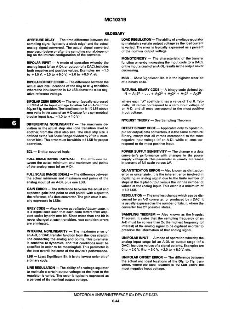
APERTURE DELAY - The time difference between the<br />
sampling signal (typically a clock edge) and the actual<br />
analog signal converted. The actual signal converted<br />
may occur before or after the sampling signal, depending<br />
on the internal configuration of the converter.<br />
BIPOLAR INPUT - A mode of operation whereby the<br />
analog input (of an A-D), or output (of a DAC), includes<br />
both negative and positive values. Examples are -1.0<br />
to + 1.0 V, -5.0 to +5.0 V, -2.0 to +8.0 V, etc.<br />
BIPOLAR OFFSET ERROR - The difference between the<br />
actual and ideal locations of the OOH to 01 H transition,<br />
where the ideal location is 1/2 LSB above the most negative<br />
reference voltage.<br />
BIPOLAR ZERO ERROR - The error (usually expressed<br />
in LSBs) of the input voltage location (of an A-D) of the<br />
SOH t081H transition. The ideal location is 1/2 LSB above<br />
zero volts in the case of an A-D setup for a symmetrical<br />
bipolar input (e.g., -1.0 to + 1.0 V).<br />
DIFFERENTIAL NONLINEARITY - The maximum. deviation<br />
in the actual step size (one transition level to<br />
another) from the ideal step size. The ideal step size is<br />
defined as the Full Scale Range divided by 2n (n = number<br />
of bits). This error must be within ± 1 LSB for proper<br />
operation.<br />
ECL - Emitter coupled logic.<br />
FULL SCALE RANGE (ACTUAL) - The difference between·<br />
the actual minimum and maximum end points<br />
of the analog input (of an A-D).<br />
FULL SCALE RANGE (IDEAL) - The difference between<br />
the actual minimum and maximum end points of the<br />
analog input (of an A-D), plus one LSB.<br />
GAIN ERROR - The difference between the actual and<br />
expected gain (end point to end point), with respect to<br />
the reference, of a data converter. The gain error is usually<br />
expressed in LSBs.<br />
GREY CODE - Also known as reflected binary code, it<br />
is a digital code such that each code differs from adjacent<br />
codes by only one bit. Since more than one bit is<br />
never changed at each transition, race condition errors<br />
are eliminated.<br />
INTEGRAL NONLINEARITY - The maximum error of<br />
an A-D, or DAC, transfer function from the ideal straight<br />
line connecting the analog end points. This parameter<br />
is sensitive to dynamics, and test conditions must be<br />
speCified in order to be meaningfull. This parameter is<br />
the best overall indicator of the device's performance.<br />
LSB - Least Significant Bit. It is the lowest order bit of<br />
a binary code.<br />
UNE REGULATION - The ability of a voltage regulator<br />
to maintain a certain output voltage as the input to the<br />
regulator is varied. The error is typically expressed as<br />
a percent of the nominal output voltage.<br />
MC10319<br />
GLOSSARY<br />
LOAD REGULATION - The ability of a voltage regulator<br />
to maintain a certain output voltage as the load current<br />
is varied. The error is typically expressed as a percent<br />
of the nominal output voltage.<br />
MONOTONICITY - The characteristic of the transfer<br />
function whereby increasing the input code (of a DAC),<br />
orthe inputsignal (ofan A-D), results in the output never<br />
decreasing.<br />
MSB - Most Significant Bit. It is the highest order bit<br />
of a binary code.<br />
NATURAL BINARY CODE - A binary code defined by:<br />
N = An2n + ... + A323 + A222 + A121 + A020<br />
where each U AU coefficient has a value of 1 or O. Typically,<br />
all zeroes correspond to a zero input voltage of<br />
an A-D, and all ones correspond to the most positive<br />
input voltage.<br />
NYQUIST THEORY - See Sampling Theorem.<br />
MOTOROLA LINEAR/INTERFACE ICs DEVICE DATA<br />
6-44<br />
OFFSET BINARY CODE - Applicable only to bipolar input<br />
(or output) data converters, it is the same as Natural<br />
Binary, except that all zeroes correspond to the most<br />
negative input voltage (of an A-D), while all ones correspond<br />
to the most positive input.<br />
POWER SUPPLY SENSITIVITY - The change in a data<br />
converter's performance with changes in the power<br />
supply voltage(s). This parameter is usually expressed<br />
in percent of full scale versus t!N.<br />
QUANTITIZATION ERROR - Also known as digitization<br />
error or uncertainty. It is the inherent error involved in<br />
digitizing an analog signal due to the finite number of<br />
steps at the digital output versus the infinite number of<br />
values at the analog input. This error is a minimum of<br />
±1/2 LSB.<br />
RESOLUTION - The smallest change which can be discerned<br />
by an A-D converter, or produced by a DAC. It<br />
is usually expressed as the number of bits, n, where the<br />
converter has 2n possible states.<br />
SAMPLING THEOREM - Also known as the Nyquist<br />
Theorem. It states that the sampling frequency of an<br />
A-D must be no less than 2x the highest frequency (of<br />
interest) of the analog signal to be digitized in order to<br />
preserve the information of that analog signal.<br />
UNIPOLAR INPUT - A mode of operation whereby the<br />
analog input range (of an A-D), or output range (of a<br />
DAC), includes values of a signal polarity. Examples are<br />
o to +2.0 V, 0 to -5.0 V, +2.0 to +8.0 V, etc.<br />
UNIPOLAR OFFSET ERROR - The difference between<br />
the actual and ideal locations of the OOH to 01 H transition,<br />
where the ideal location is 1/2 LSB above the<br />
most negative input voltage.


