Voltage References
Voltage References
Voltage References

You also want an ePaper? Increase the reach of your titles
YUMPU automatically turns print PDFs into web optimized ePapers that Google loves.
Auto Gray Scale Control Loops<br />
This section supplies current drives to the RGB cathode<br />
amplifiers and receives a signal feedback from them,<br />
proportional to the combined cathode currents. The current<br />
feedback is used to establish a set of feedback loops to<br />
control the DC and gain of the RGB drives. There are three<br />
loops to control the dark currents and another three to control<br />
the gains. During the field blanking period the video outputs<br />
are switched off and a set of references are inserted on three<br />
consecutive lines to control the R, G, and B outputs<br />
respectively. The white current reference pulses are sent first,<br />
followed by the black current reference pulses. Drives whose<br />
outputs are not being monitored are rendered nonconducting<br />
during this time.<br />
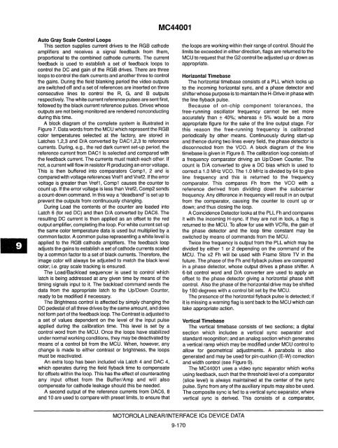
A block diagram of the complete system is illustrated in<br />
Figure 7. Data words from the MCU which represent the RGB<br />
color temperatures selected at the factory, are stored in<br />
Latches 1,2,3 and D/A converted by DAC1 ,2,3 to reference<br />
currents. During, e.g., the red dark current set-up period, the<br />
reference current from DAC1 is selected and compared with<br />
the feedback current. The currents must match each other. If<br />
not, a current will flow in resistor R producing an error voltage.<br />
This is then buffered into comparators Comp1, 2 and is<br />
compared with voltage references Vref1 and Vref2. If the error<br />
voltage is greater than Vref1, Comp1 causes the counter to<br />
count up. If the error voltage is less than Vref2, Comp2 sends<br />
a count-down command. In this way a "deadband" is set up to<br />
prevent the outputs from continuously changing.<br />
During Load the contents of the counter are loaded into<br />
Latch 6 (for red DC) and then D/A converted by DAC6. The<br />
resulting DC current is then applied as an offset to the red<br />
output amplifier, completing the loop. For white current set-up<br />
the same color temperature data is used but multiplied by a<br />
common factor. A common pulse representing a white level is<br />
applied to the RGB cathode amplifiers. The feedback loop<br />
adjusts the gains to establish a set of cathode currents scaled<br />
by a common factor to a set of black currents. Therefore, the<br />
image color will always be adjusted to match the black level<br />
color; i.e. gray scale tracking is ensured.<br />
The Load/Backload sequencer is used to control which<br />
latch is being addressed at any given time by means of the<br />
timing signals input to it. The backload command sends the<br />
data from the appropriate latch to the Up/Down Counter,<br />
ready to be modified if necessary.<br />
The Brightness control is affected by simply changing the<br />
DC pedestal of all three drives by the same amount, and does<br />
notfarm part of the feedback loop_ The Contrast is adjusted to<br />
a set of values dependent on the level of the input pulse<br />
applied during the calibration time. This level is set by a<br />
control word from the MCU. Once the loops have stabilized<br />
under normal working conditions, they may be deactivated by<br />
means of a control bit from the MCU. When, however, any<br />
change is made to either contrast or brightness, the loops<br />
must be reactivated.<br />
An extra loop has been included via Latch 4 and DAC 4,<br />
which operates during the field flyback time to compensate<br />
for offsets within the loop. This has the effect of counteracting<br />
any input offset from the Buffer/Amp and will also<br />
compensate for cathode leakage should this be needed.<br />
A second output of the reference currents from DAC6, 8<br />
and 10 are used to compare with preset limits, to ensure that<br />
MC44001<br />
MOTOROLA LINEAR/INTERFACE ICs DEVICE DATA<br />
9-170<br />
the loops are working within their range of control. Should the<br />
limits be exceeded in either direction, flags are returned to the<br />
MCU to request that the G2 control be adjusted up or down as<br />
appropriate.<br />
Horizontal Timebase<br />
The horizontal timebase consists of a PLL which locks up<br />
to the incoming horizontal sync, and a phase detector and<br />
shifter whose purpose is to maintain the H-Drive in phase with<br />
the line flyback pulse.<br />
Because of on-chip component tolerances, the<br />
free-running oscillator frequency cannot be set more<br />
accurately than ± 40%; whereas ± 5% would be a more<br />
appropriate figure for the sake of the line output stage. For<br />
this reason the free-running frequency is calibrated<br />
periodically by other means. Continuously during start-up<br />
and thence during two lines every field, the phase detector is<br />
disconnected from the VCO. A block diagram of the line<br />
timebase is given in Figure 8. The calibration loop consists of<br />
a frequency comparator driving an Up/Down Counter. The<br />
count is D/A converted to give a DC bias which is used to<br />
correct a 1.0 MHz VCO. The 1.0 MHz is divided by 64 to give<br />
line frequency and this is returned to the frequency<br />
comparator. This compares Fh from the VCO with a<br />
reference derived from dividing down the subcarrier<br />
frequency. Any difference in frequency will result in an output<br />
from the comparator, causing the counter to count up or<br />
down; and thus closing the loop.<br />
A Coincidence Detector looks at the PLL Fh and compares<br />
it with the incoming H-sync. If they are not in lock, a flag is<br />
returned to the MCU. To allow for use with VCRs, the gain of<br />
the phase detector and the loop time constant may be<br />
switched by means of commands from the MCU.<br />
Twice line frequency is output from the PLL which may be<br />
divided by either 1 or 2 depending on the command of the<br />
MCU. The x2 Fh will be used with Frame Store TV in the<br />
future. The phase of the Fh and fiyback pulses are compared<br />
in a phase detector, whose output drives a phase shifter. A<br />
6-bit control word and D/A converter are used to apply an<br />
offset to Ihe phase detector giving a horizontal phase shift<br />
control. Also the phase of the horizontal drive may be shifted<br />
by 180 degrees with a control bit set by the MCU.<br />
The presence of the horizontal flyback pulse is detected; if<br />
it is missing a warning flag is sent back to the MCU which can<br />
take appropriate action.<br />
Vertical Timebase<br />
The vertical timebase consists of two sections; a digital<br />
section which includes a vertical sync separator and<br />
standard recognition; and an analog section which generates<br />
a vertical ramp which may be modified under MCU control to<br />
allow for geometrical adjustments. A parabola is also<br />
generated and may be used for pin-cushion (E-W) correction<br />
and width control (see Figure 9).<br />
The MC44001 uses a video sync separator which works<br />
using feedback, such that the threshold level of a comparator<br />
(slice level) is always maintained at the center of the sync<br />
pulse. Sync from any of the auxiliary inputs may also be used.<br />
The composite sync is fed to a vertical sync separator, where<br />
vertical sync is derived. This consists of a comparator,