Voltage References
Voltage References
Voltage References

Create successful ePaper yourself
Turn your PDF publications into a flip-book with our unique Google optimized e-Paper software.
Introduction<br />
The MC1388 is a multi-frequency capable integrated<br />
circuit used for geometry correction in monitors and HDTV<br />
receivers. With a few inputs the MC1388 will provide ten<br />
functions, eight with complements, as output waveforms.<br />
These waveforms can then be used by the control circuitry<br />
in any combination to modulate the horizontal and vertical<br />
deflection currents for geometry correction.<br />
The MC1388 accomplishes multi-frequency operation by<br />
allowing external components to determine the nominal<br />
frequency of operation. This is done by choosing<br />
resistor-capacitor pairs for the desired horizontal and vertical<br />
oscillator frequencies. The horizontal and vertical sync<br />
inputs then provide the timing reference to which the output<br />
waveforms of the MC1388 adhere.<br />
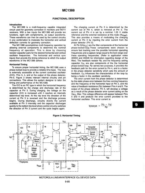
Horizontal Timing<br />
To ensure proper horizontal timing, the MC1388 uses a<br />
phase-locked-loop to provide a reliable time base. The loop<br />
is externally accessible at the current controlled oscillator<br />
(ICO), Pins 3, 4, and at the output of the phase detector,<br />
Pin 5. Figure 2 shows relevant internal circuitry and pin<br />
connections. This allows the system designer to tailor the<br />
timing and performance of the MC1388.<br />
The ICO is an RC type in which the horizontal frequency<br />
is determined by the charge and discharge rate of the<br />
capacitor at Pin 3. During charging, the voltage on the<br />
capacitor (CH) is increased until it reaches an internally<br />
determined trip level. At this trip level the direction of the<br />
current at Pin 3 is reversed and the discharge process<br />
begins. During discharge, circuitry diverts the current<br />
available at Pin 3 internally and the capacitor discharges<br />
quickly to the bottom trip level where control circuitry switches<br />
the direction of Pin 3 current and the cycle begins again.<br />
L ________ :J<br />
* Polyslyrene<br />
4<br />
R<br />
MC1388<br />
FUNCTIONAL DESCRIPTION<br />
Figure 2. Horizontal Timing<br />
---- ----,<br />
I 10kQ Hpll I<br />
I 11lF ::f---J' Filler I<br />
I - 0.01 I<br />
L _________ ...l<br />
MOTOROLA LINEAR/INTERFACE ICs DEVICE DATA<br />
9-85<br />
The charging current at Pin 3 is determined by the<br />
current out of Pin 4, which is mirrored at Pin 3. The<br />
current out of Pin 4 is set by a nominal 1.25 V stable<br />
reference and the external resistance at this node (RHset).<br />
This also provides a means of modulating the charging<br />
current at Pin 3 by injecting the error current from the<br />
phase detector (Pin 5).<br />
At Pin 5(HpLLl are the filter components of the horizontal<br />
phase-locked-loop. These components were chosen to<br />
ensure fast tracking over the possible horizontal operating<br />
frequencies and a capture range equal to the lock range over<br />
these operating frequencies. (Refer to application notes<br />
AN553 and AN535 for information regarding design of the<br />
filter). The feedback resistor RF, and the frequency setting<br />
capacitor CH, are also components of the the horizontal<br />
phase-locked-loop. RF serves two purposes, it provides the<br />
feedback path for the error current to Pin 4, and is a factor<br />
in the phase detector sensitivity which sets the amount of<br />
feedback. CH influences the characteristics of the loop by<br />
being a factor in the oscillator sensitivity.<br />
The error current from the phase detector is determined<br />
by the static phase error between the free running frequency<br />
and the frequency of the horizontal input at Pin 2, and the<br />
value of feedback resistance (RF) between Pins 4 and 5. The<br />
output of the phase detector, Pin 5, will develop a voltage<br />
as a result of the phase detector error current acting on the<br />
HPLL filter. This voltage difference will appear between Pins<br />
5 and 4 and produce the error current provided to the<br />
horizontal oscillator. This error current is:<br />
IERROR = (V5 - V4)<br />
RF<br />
I<br />
I<br />
I<br />
I<br />
I<br />
I<br />
__ .J