Voltage References
Voltage References
Voltage References
You also want an ePaper? Increase the reach of your titles
YUMPU automatically turns print PDFs into web optimized ePapers that Google loves.
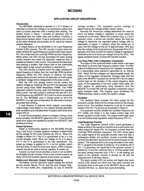
Introduction<br />
The MC33092, designed to operate in a 12 V system, is<br />
intended to control the voltage in an automotive system that<br />
uses a 3 phase alternator with a rotating field winding. The<br />
system shown in Figure 1 includes an alternator with its<br />
associated field coil, stator coils and rectifiers, a battery, a<br />
lamp and an ignition switch. A tap is connected to one corner<br />
of the stator windings and provides an AC signal for rotation<br />
(phase) detection.<br />
A unique feature of the MC33092 is the Load Response<br />
Control (LRC) circuitry. The LRC circuitry is active when the<br />
stator winding AC signal frequency (phase buffer input signal,<br />
Pin 10) is lower than the Low/High RPM transition frequency.<br />
When active, the LRC circuitry dominates the basic analog<br />
control circuitry and slows the alternator response time to<br />
sudden increases in load current. This prevents the alternator<br />
from placing a sudden, high torque load on the automobile<br />
engine when a high current accessory is switched on.<br />
The LRC circuitry is inactive when the stator winding AC<br />
signal frequency is higher than the Low/High RPM transition<br />
frequency. When the LRC circuitry is inactive, the basic<br />
analog control circuitry controls the alternator so it will supply<br />
a constant voltage that is independent of the load current.<br />
Both the LRC and analog control circuits control the<br />
system voltage by switching ON and OFF the alternator field<br />
current using Pulse Width Modulation (PWM). The PWM<br />
approach controls the duty cycle and therefore the average<br />
field current. The field current is switched ON and OFF at a<br />
fixed frequency by a MOSFET (01 ) which is driven directly by<br />
the IC. The MC33092 uses a charge pump to drive the<br />
MOSFET in a high side configuration for alternators having a<br />
grounded field winding.<br />
A fault detector is featured which detects overvoltage,<br />
undervoltage, slow rotation or non-rotation (broken alternator<br />
belt) conditions and indicates them through a fault lamp drive<br />
output (Pin 4).<br />
A Load Dump protection circuit is included. During a load<br />
dump condition, the MOSFET gate drive (Pin 17) and the fault<br />
lamp drive output are disabled to protect the MOSFET, field<br />
winding and lamp.<br />
Power-Up/Down<br />
Power is continuously applied to the MC33092 through<br />
VCC1 and VCC3. A power-up/down condition is determined<br />
by the voltage on the Lamp Collector pin (Pin 3). When this<br />
voltage is below 0.5 V the IC is guaranteed to be in a low<br />
current standby mode. When the voltage at Pin 3 is above<br />
2.0 V, the IC is guaranteed to be fully operational. The<br />
power-up voltage is applied to Pin 3 via the ignition switch<br />
and fault lamp. In case the fault lamp opens, a 500 n bypass<br />
resistor should be used to ensure regulator IC power-up.<br />
A power-up reset circuit provides a reset or set condition<br />
for all digital counter circuitry. There is also a built-in power-up<br />
delay circuit that protects against erratic power-up signals.<br />
BaHery and Alternator Output <strong>Voltage</strong> Sensing<br />
The battery and the alternator output voltage are sensed<br />
by the remote (Sense, Pin 2), and the local (Supply Reg.,<br />
Pin 12) input buffer pins, respectively, by way of external<br />
MC33092<br />
APPLICATION CIRCUIT DESCRIPTION<br />
MOTOROLA LINEAR/INTERFACE ICs DEVICE DATA<br />
10-60<br />
voltage dividers. The regulated system voltage is<br />
determined by the voltage divider resistor values.<br />
Normally the remote pin voltage determines the value at<br />
which the battery voltage is regulated. In some cases the<br />
remote pin is not used. When this condition (VPin 2 < 0.6 V<br />
typically) exists, a sense loss function allows the local pin<br />
voltage to determine the regulated battery voltage with no<br />
attenuation of signal. If, however, when the remote pin is<br />
used, and the voltage at this pin is approximately 25% less<br />
than the voltage at the local sense pin (but greater than 0.6 V,<br />
typically), the value at which the battery voltage is regulated is<br />
switched to the local sense pin voltage (minus the 25%). The<br />
signal combiner/switch controls this transfer function.<br />
Low Pass Filter, DAC & Regulator Comparator<br />
The output of the combiner/switch buffer feeds a low pass<br />
filter block to remove high frequency system noise. The filter<br />
output is buffered and compared by the regulator comparator<br />
to a descending ramp waveform generated by an internal<br />
DAC. When the two voltages are approximately equal, the<br />
output of the regulator comparator changes state and the<br />
gate of the MOSFET is pulled low (turned OFF) by the output<br />
control logic for the duration of the output frequency clock<br />
cycle. At the beginning of the next output clock cycle, the<br />
DAC begins its descending ramp waveform and the<br />
MOSFET is turned ON until the regulator comparator output<br />
again changes state. This ongoing cycle constitutes the<br />
PWM technique used to control the system voltage.<br />
Oscillator<br />
The oscillator block provides the clock pulses for the<br />
prescaler-counter chain and the charge control for the charge<br />
pump circuit. The oscillator frequency is set by an external<br />
resistor from Pin 7 to ground as presented in Figure 6.<br />
The prescaler-counter divides the oscillator frequency by<br />
212 (4096) and feeds it to the output control logic and<br />
divider-up/down counter chain. The output control logic uses<br />
it as the fundamental regulation output frequency (Pin 17).<br />
Load Response Control<br />
The Load Response Control (LRC) circuit generates a<br />
digital control of the regulation function and is active when the<br />
stator output AC signal (Pin 10) frequency is lower than the<br />
Low/High RPM transition frequency. The LRC circuit takes<br />
the output signal of the prescaler-counter chain and with a<br />
subsequent divider and up/down counter to provide delay,<br />
controls the alternator response time to load increases on the<br />
system. The response time is pin programmable to two rates.<br />
Pin 11 programs the divider to divide by 12 or divide by 48. If<br />
Pin 11 is grounded, the signal fed to the up/down counter is<br />
divided by 12 and the response time is 12 times slower than<br />
the basic analog response time. If Pin 11 is left floating, the<br />
signal to the up/down counter is divided by 48 and the<br />
response time is 48 times slower.<br />
The basic analog (LRC not active) and digital duty cycle<br />
control (LRC active) are OR'd such that either function will<br />
terminate drive to the gate of the MOSFET device with the<br />
shortest ON-time, i.e., lower duty cycle dominating.


