Voltage References
Voltage References
Voltage References
Create successful ePaper yourself
Turn your PDF publications into a flip-book with our unique Google optimized e-Paper software.
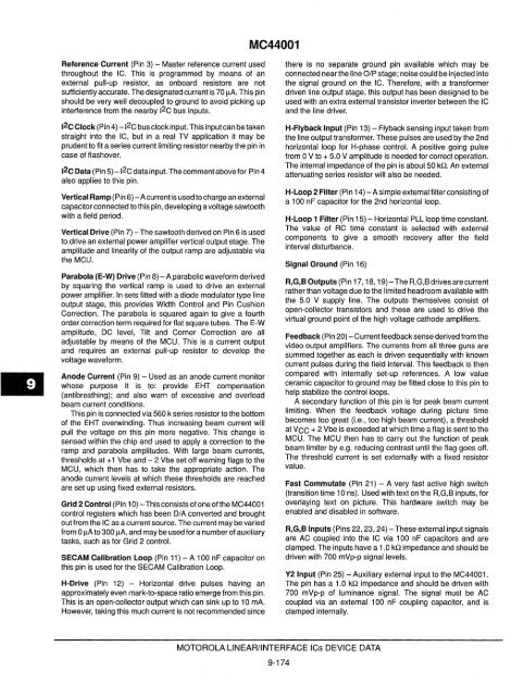
Reference Current (Pin 3) - Master reference current used<br />
throughout the IC. This is programmed by means of an<br />
external pull-up resistor, as onboard resistors are not<br />
sufficiently accurate. The designated current is 70 !LA. This pin<br />
should be very well decoupled to ground to avoid picking up<br />
interference from the nearby 12C bus inputs.<br />
12C Clock (Pin 4) -12C bus clock input. This input can be taken<br />
straight into the IC, but in a real TV application it may be<br />
prudent to fit a series current limiting resistor nearby the pin in<br />
case of flashover.<br />
12C Data (Pin 5) -12C data input. The comment above for Pin 4<br />
also applies to this pin.<br />
Vertical Ramp (Pin 6) -A current is used to charge an external<br />
capacitor connected to this pin, developing a voltage sawtooth<br />
with a field period.<br />
Vertical Drive (Pin 7) - The sawtooth derived on Pin 6 is used<br />
to drive an external power amplifier vertical output stage. The<br />
amplitude and linearity of the output ramp are adjustable via<br />
the MCU.<br />
Parabola (E-W) Drive (Pin 8) - A parabolic waveform derived<br />
by squaring the vertical ramp is used to drive an external<br />
power amplifier. In sets fitted with a diode modulator type line<br />
output stage, this provides Width Control and Pin Cushion<br />
Correction. The parabola is squared again to give a fourth<br />
order correction term required for flat square tubes. The E-W<br />
amplitude, DC level, Tilt and Corner Correction are all<br />
adjustable by means of the MCU. This is a current output<br />
and requires an external pull-up resistor to develop the<br />
voltage waveform.<br />
Anode Current (Pin 9) - Used as an anode current monitor<br />
whose purpose it is to: provide EHT compensation<br />
(antibreathing); and also warn of excessive and overload<br />
beam current conditions.<br />
This pin is connected via 560 k series resistor to the bottom<br />
of the EHT overwinding. Thus increasing beam current will<br />
pull the voltage on this pin more negative. This change is<br />
sensed within the chip and used to apply a correction to the<br />
ramp and parabola amplitudes. With large beam currents,<br />
thresholds at + 1 Vbe and - 2 Vbe set off warning flags to the<br />
MCU, which then has to take the appropriate action. The<br />
anode current levels at which these thresholds are reached<br />
are set up using fixed external resistors.<br />
Grid 2 Control (Pin 10) - This consists of one ofthe MC44001<br />
control registers which has been D/A converted and brought<br />
out from the IC as a current source. The current may be varied<br />
from o !LA to 300 !LA, and may be used for a number of auxiliary<br />
tasks, such as for Grid 2 control.<br />
SECAM Calibration Loop (Pin 11) - A 100 nF capacitor on<br />
this pin is used for the SECAM Calibration Loop.<br />
H-Drive (Pin 12) - Horizontal drive pulses having an<br />
approximately even mark-to-space ratio emerge from this pin.<br />
This is an open-collector output which can sink up to 10 mAo<br />
However, taking this much current is not recommended since<br />
MC44001<br />
there is no separate ground pin available which may be<br />
connected near the line O/P stage; noise could be injected into<br />
the signal ground on the IC. Therefore, with a transformer<br />
driven line output stage, this output has been designed to be<br />
used with an extra external transistor inverter between the IC<br />
and the line driver.<br />
H-Flyback Input (Pin 13) - Flyback sensing input taken from<br />
the line output transformer. These pulses are used by the 2nd<br />
horizontal loop for H-phase control. A positive going pulse<br />
from 0 V to + 5.0 V amplitude is needed for correct operation.<br />
The internal impedance of the pin is about 50 kQ. An external<br />
attenuating series resistor will also be needed.<br />
H-Loop 2 Filter (Pin 14) - A simple external filter consisting of<br />
a 100 nF capacitor for the 2nd horizontal loop.<br />
H-Loop 1 Filter (Pin 15) - Horizontal PLL loop time constant.<br />
The value of RC time constant is selected with external<br />
components to give a smooth recovery after the field<br />
interval disturbance.<br />
Signal Ground (Pin 16)<br />
MOTOROLA LINEAR/INTERFACE ICs DEVICE DATA<br />
9-174<br />
R,G,B Outputs (Pin 17, 18, 19)-The R,G,Bdrives are current<br />
rather than voltage due to the limited headroom available with<br />
the 5.0 V supply line. The outputs themselves consist of<br />
open-collector transistors and these are used to drive the<br />
virtual ground point of the high voltage cathode amplifiers.<br />
Feedback (Pin 20) - Current feedback sense derived from the<br />
video output amplifiers. The currents from all three guns are<br />
summed together as each is driven sequentially with known<br />
current pulses during the field interval. This feedback is then<br />
compared with internally set-up references. A low value<br />
ceramic capacitor to ground may be fitted close to this pin to<br />
help stabilize the control loops.<br />
A secondary function of this pin is for peak beam current<br />
limiting. When the feedback voltage during picture time<br />
becomes too great (i.e., too high beam current), a threshold<br />
at VCC + 2 Vbe is exceeded at which time a flag is sent to the<br />
MCU. The MCU then has to carry out the function of peak<br />
beam limiter by e.g. reducing contrast until the flag goes off.<br />
The threshold current is set externally with a fixed resistor<br />
value.<br />
Fast Commutate (Pin 21) - A very fast active high switch<br />
(transition time IOns). Used with text on the R,G,B inputs, for<br />
overlaying text on picture. This hardware switch may be<br />
enabled and disabled in software.<br />
R,G,B Inputs (Pins 22, 23, 24) - These external input signals<br />
are AC coupled into the IC via 100 nF capacitors and are<br />
clamped. The inputs have a 1.0 kQ impedance and should be<br />
driven with 700 mVp-p signal levels.<br />
Y2 Input (Pin 25) - Auxiliary external input to the MC44001.<br />
The pin has a 1.0 kQ impedance and should be driven with<br />
700 mVp-p of luminance signal. The signal must be AC<br />
coupled via an external 100 nF coupling capacitor, and is<br />
clamped internally.


