T EVIS i - AmericanRadioHistory.Com
T EVIS i - AmericanRadioHistory.Com
T EVIS i - AmericanRadioHistory.Com

You also want an ePaper? Increase the reach of your titles
YUMPU automatically turns print PDFs into web optimized ePapers that Google loves.
I<br />
voltage regulation', '.'. as well and gives<br />
promise of application in special -purpose<br />
trigger and switching circuits.<br />
Nothing has appeared previously on the<br />
direct use of the germanium diode as a<br />
negative -resistance amplifier, although<br />
Dowell' and Becker, Green, and Pearson'<br />
have called attention to the application<br />
of another semiconductor device<br />
-the thermistor -as a negative- resistance<br />
amplifier.<br />
Applications<br />
Several interesting and provocative<br />
applications of the negative -resistance<br />
phenomenon, and of effects in and<br />
around the region of zero dynamic resistance,<br />
are possible. Figures 3 to 6<br />
illustrate some of the possible applications.<br />
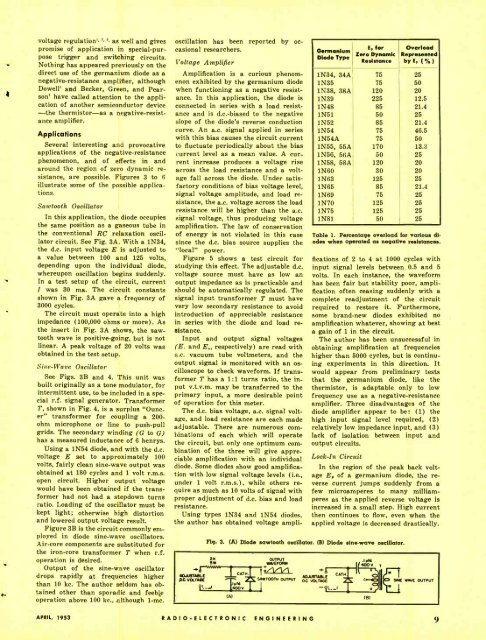
Sawtooth Oscillator<br />
In this application, the diode occupies<br />
the same position as a gaseous tube in<br />
the conventional RC relaxation oscillator<br />
circuit. See Fig. 3A. With a 1N34,<br />
the d.c. input voltage E is adjusted to<br />
a value between 100 and 125 volts,<br />
depending upon the individual diode,<br />
whereupon oscillation begins suddenly.<br />
In a test setup of the circuit, current<br />
I was 30 ma. The circuit constants<br />
shown in Fig. 3A gave a frequency of<br />
3000 cycles.<br />
The circuit must operate into a high<br />
impedance (100,000 ohms or more). As<br />
the insert in Fig. 3A shows, the saw -<br />
tooth wave is positive -going, but is not<br />
linear. A peak voltage of 20 volts was<br />
obtained in the test setup.<br />
Sine -Wave Oscillator<br />
See Figs. 3B and 4. This unit was<br />
built originally as a tone modulator, for<br />
intermittent use, to be included in a special<br />
r.f. signal generator. Transformer<br />
T, shown in Fig. 4, is a surplus "Ouncer"<br />
transformer for coupling a 200 -<br />
ohm microphone or line to push -pull<br />
grids. The secondary winding (G to G)<br />
has a measured inductance of 6 henrys.<br />
Using a 1N54 diode, and with the d.c.<br />
voltage E set to approximately 100<br />
volts, fairly clean sine -wave output was<br />
obtained at 180 cycles and 1 volt r.m.s.<br />
open circuit. Higher output voltage<br />
would have been obtained if the transformer<br />
had not had a stepdown turns<br />
ratio. Loading of the oscillator must be<br />
kept light; otherwise high distortion<br />
and lowered output voltage result.<br />
Figure 3B is the circuit commonly employed<br />
in diode sine -wave oscillators.<br />
Air -core components are substituted for<br />
the iron -core transformer T when r.f.<br />
operation is desired.<br />
Output of the sine -wave oscillator<br />
drops rapidly at frequencies higher<br />
than 10 kc. The author seldom has obtained<br />
other than sporadic and feeble<br />
operation above 100 kc., although 1 -mc.<br />
oscillation has been reported by occasional<br />
researchers.<br />
Voltage Amplifier<br />
Amplification is a curious phenomenon<br />
exhibited by the germanium diode<br />
when functioning as a negative resistance.<br />
In this application, the diode is<br />
connected in series with a load resistance<br />
and is d.c.-biased to the negative<br />
slope of the diode's reverse conduction<br />
curve. An a.c. signal applied in series<br />
with this bias causes the circuit current<br />
to fluctuate periodically about the bias<br />
current level as a mean value. A current<br />
increase produces a voltage rise<br />
across the load resistance and a voltage<br />
fall across the diode. Under satisfactory<br />
conditions of bias voltage level,<br />
signal voltage amplitude, and load resistance,<br />
the a.c. voltage across the load<br />
resistance will be higher than the a.c.<br />
signal voltage, thus producing voltage<br />
amplification. The law of conservation<br />
of energy is not violated in this case<br />
since the d.c. bias source supplies the<br />
"local" power.<br />
Figure 5 shows a test circuit for<br />
studying this effect. The adjustable d.c.<br />
voltage source must have as low an<br />
output impedance as is practicable and<br />
should be automatically regulated. The<br />
signal input transformer T must have<br />
very low secondary resistance to avoid<br />
introduction of appreciable resistance<br />
in series with the diode and load resistance.<br />
Input and output signal voltages<br />
(E, and E respectively) are read with<br />
a.c. vacuum tube voltmeters, and the<br />
output signal is monitored with an oscilloscope<br />
to check waveform. If transformer<br />
T has a 1:1 turns ratio, the input<br />
v.t.v.m. may be transferred to the<br />
primary input, a more desirable point<br />
of operation for this meter.<br />
The d.c. bias voltage, a.c. signal voltage,<br />
and load resistance are each made<br />
adjustable. There are numerous combinations<br />
of each which will operate<br />
the circuit, but only one optimum combination<br />
of the three will give appreciable<br />
amplification with an individual<br />
diode. Some diodes show good amplification<br />
with low signal voltage levels (i.e.,<br />
under 1 volt r.m.s.), while others require<br />
as much as 10 volts of<br />
t<br />
signal with<br />
proper adjustment of d.c. bias and load<br />
resistance.<br />
Using types 1N34 and 1N54 diodes,<br />
the author has obtained voltage ampli-<br />
2K<br />
OUTPUT<br />
5<br />
WAVEFORM<br />
CAT H<br />
ADJUSTABLE<br />
QC VOLTAGE<br />
SAWTOOTH OUTPUT<br />
Iy,d<br />
-J 400 v<br />
Germanium<br />
Diode Type<br />
E1, for<br />
Zero Dynamic<br />
Resistance<br />
Overload<br />
Represented<br />
by E, (%)<br />
1N34, 34A 75 25<br />
1N35 75 50<br />
1N38, 38A 120 20<br />
1N39 225 12.5<br />
1N48 85 21.4<br />
1N51 50 25<br />
1N52 85 21.4<br />
1N54 75 46.5<br />
1N54A 75 50<br />
1N55, 55A 170 13.3<br />
1N56, 56A 50 25<br />
1N58, 58A 120 20<br />
1N60 30 20<br />
1N63 125 25<br />
1N65 85 21.4<br />
1N69 75 25<br />
1N70 125 25<br />
1N75 125 25<br />
1N81 50 25<br />
Table 1. Percentage overload for various diodes<br />
when operated as negative resistances.<br />
fications of 2 to 4 at 1000 cycles with<br />
input signal levels between 0.5 and 5<br />
volts. In each instance, the waveform<br />
has been fair but stability poor, amplification<br />
often ceasing suddenly with a<br />
complete readjustment of the circuit<br />
required to restore it. Furthermore,<br />
some brand -new diodes exhibited no<br />
amplification whatever, showing at best<br />
a gain of 1 in the circuit.<br />
The author has been unsuccessful in<br />
obtaining amplification at frequencies<br />
higher than 5000 cycles, but is continuing<br />
experiments in this direction. It<br />
would appear from preliminary tests<br />
that the germanium diode, like the<br />
thermistor, is adaptable only to low<br />
frequency use as a negative -resistance<br />
amplifier. Three disadvantages of the<br />
diode amplifier appear to be: (1) the<br />
high input signal level required, (2)<br />
relatively low impedance input, and (3)<br />
lack of isolation between input and<br />
output circuits.<br />
Lock -In Circuit<br />
In the region of the peak back voltage<br />
E, of a germanium diode, the reverse<br />
current jumps suddenly from a<br />
few microamperes to many milliamperes<br />
as the applied reverse voltage is<br />
increased in a small step. High current<br />
then continues to flow, even when the<br />
applied voltage is decreased drastically.<br />
Fig. 3. (A) Diode sawtooth oscillator. (B) Diode sine -wave oscillator.<br />
(A)<br />
ADJUSTABLE<br />
DC VOLTAGE<br />
C AT H<br />
yid<br />
400 v<br />
IRI<br />
SUNS WAVE OUTPUT<br />
APRIL, 1953 RADIO -ELECTRONIC ENGINEERING t