CME34M Hardware Manual - RTD Embedded Technologies, Inc.
CME34M Hardware Manual - RTD Embedded Technologies, Inc.
CME34M Hardware Manual - RTD Embedded Technologies, Inc.

You also want an ePaper? Increase the reach of your titles
YUMPU automatically turns print PDFs into web optimized ePapers that Google loves.
Advanced Digital I/O Ports (aDIO)<br />
This board supports 12 bits of TTL/CMOS compatible digital I/O (TTL signaling). These I/O lines are grouped<br />
into two ports, Port 0 and Port 1. Port 0 is bit programmable; Port 1 is byte programmable. Port 0 supports <strong>RTD</strong>’s<br />
Advanced Digital Interrupt modes. The three modes are strobe, match and event. Strobe mode generates an<br />
interrupt and latches Port 0 when the strobe input transitions from low to high. Match mode generates an<br />
interrupt when an 8-bit pattern is received in parallel that matches the match mask register. Event mode<br />
generates an interrupt when a change occurs on any bit. In any mode, masking can be used to monitor selected<br />
lines.<br />
When the CPU boots, all digital I/O lines are programmed as inputs, meaning that the digital I/O line’s initial<br />
state is undetermined. If the digital I/O lines must power up to a known state, an external 10 kΩ resistor must<br />
be added to pull the line high or low.<br />
The 8-bit control read/write registers for the digital I/O lines are located from I/O address 9C0h to 9C4h. These<br />
registers are written to zero upon power up. From 9C0h to 9C4h, the name of these registers are Port 0 data,<br />
Port 1 data, Multi-Function, DIO-Control, and Wake Control register.<br />
Note <strong>RTD</strong> provides drivers that support the aDIO interface on popular operating systems. <strong>RTD</strong><br />
recommends using these drivers instead of accessing the registers directly.<br />
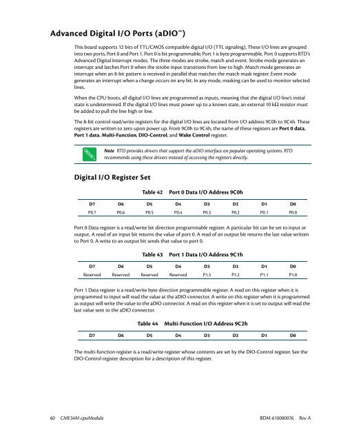
Digital I/O Register Set<br />
Table 42<br />
Port 0 Data I/O Address 9C0h<br />
D7 D6 D5 D4 D3 D2 D1 D0<br />
P0.7 P0.6 P0.5 P0.4 P0.3 P0.2 P0.1 P0.0<br />
Port 0 Data register is a read/write bit direction programmable register. A particular bit can be set to input or<br />
output. A read of an input bit returns the value of port 0. A read of an output bit returns the last value written<br />
to Port 0. A write to an output bit sends that value to port 0.<br />
Table 43<br />
Port 1 Data I/O Address 9C1h<br />
D7 D6 D5 D4 D3 D2 D1 D0<br />
Reserved Reserved Reserved Reserved P1.3 P1.2 P1.1 P1.0<br />
Port 1 Data register is a read/write byte direction programmable register. A read on this register when it is<br />
programmed to input will read the value at the aDIO connector. A write on this register when it is programmed<br />
as output will write the value to the aDIO connector. A read on this register when it is set to output will read the<br />
last value sent to the aDIO connector.<br />
Table 44<br />
Multi-Function I/O Address 9C2h<br />
D7 D6 D5 D4 D3 D2 D1 D0<br />
The multi-function register is a read/write register whose contents are set by the DIO-Control register. See the<br />
DIO-Control register description for a description of this register.<br />
60 <strong>CME34M</strong> cpuModule BDM-610000076 Rev A