

Complete Report - University of New South Wales
Complete Report - University of New South Wales
Complete Report - University of New South Wales

You also want an ePaper? Increase the reach of your titles
YUMPU automatically turns print PDFs into web optimized ePapers that Google loves.
4.1 INTRODUCTION TO RESEARCH<br />
Photovoltaics, the direct conversion <strong>of</strong> sunlight to electricity using solar cells, is recognised<br />
as one <strong>of</strong> the most promising options for a sustainable energy future. The ARC Photovoltaics<br />
Centre <strong>of</strong> Excellence commenced in mid-2003, drawing together previous disparate strands<br />
<strong>of</strong> work, supported under a variety <strong>of</strong> programs, into a coherent whole addressing the key<br />
challenges facing photovoltaics, as well as “spin-<strong>of</strong>f” applications in microelectronics and<br />
optoelectronics.<br />
The Centre’s photovoltaics research is divided into three interlinked strands addressing nearterm,<br />
medium-term and long-term needs, respectively. The present photovoltaic market is<br />
dominated by “fi rst-generation” product based on silicon wafers, either single-crystalline as in<br />
microelectronics, or a lower-grade multicrystalline wafer (Fig. 4.1.1). This market dominance<br />
is likely to continue for at least the next decade. First-generation production volume is growing<br />
rapidly, with the technological emphasis upon streamlining manufacturing to reduce costs<br />
while, at the same time, improving the energy conversion effi ciency <strong>of</strong> the product. Other key<br />
issues involve reducing the manufacturing spread on multicrystalline wafer lines caused by<br />
variability in wafer quality (typically 20% spread in cell output) and elimination <strong>of</strong> the effects <strong>of</strong><br />
boron-oxygen defects in both types <strong>of</strong> wafers. These defects become active under illumination<br />
and reduce the performance <strong>of</strong> most commercial modules by about 3%. They also constrain<br />
the specifi cation <strong>of</strong> the starting silicon wafer, restricting cell design possibilities. Also important<br />
is the reduction <strong>of</strong> the thickness <strong>of</strong> the starting silicon wafer without losing performance, to<br />
save on material use, and the development <strong>of</strong> low-cost techniques for reducing refl ection<br />
from multicrystalline cells.<br />
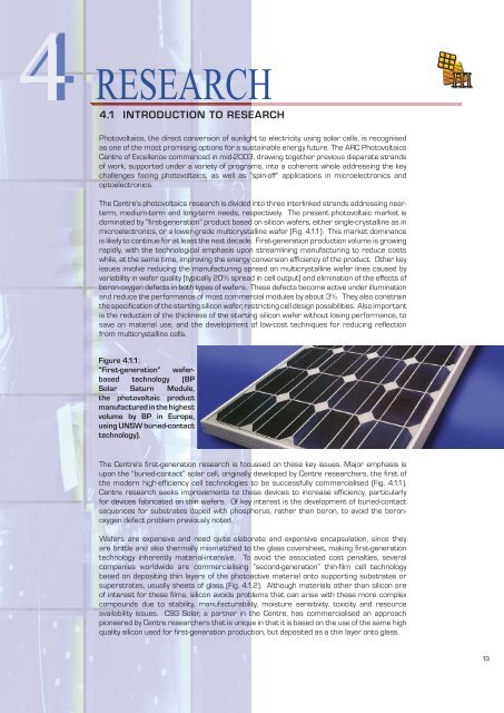
Figure 4.1.1:<br />
“First-generation” waferbased<br />
technology (BP<br />
Solar Saturn Module,<br />
the photovoltaic product<br />
manufactured in the highest<br />
volume by BP in Europe,<br />
using UNSW buried-contact<br />
technology).<br />
The Centre’s fi rst-generation research is focussed on these key issues. Major emphasis is<br />
upon the “buried-contact” solar cell, originally developed by Centre researchers, the fi rst <strong>of</strong><br />
the modern high-effi ciency cell technologies to be successfully commercialised (Fig. 4.1.1).<br />
Centre research seeks improvements to these devices to increase effi ciency, particularly<br />
for devices fabricated on thin wafers. Of key interest is the development <strong>of</strong> buried-contact<br />
sequences for substrates doped with phosphorus, rather than boron, to avoid the boronoxygen<br />
defect problem previously noted.<br />
Wafers are expensive and need quite elaborate and expensive encapsulation, since they<br />
are brittle and also thermally mismatched to the glass coversheet, making fi rst-generation<br />
technology inherently material-intensive. To avoid the associated cost penalties, several<br />
companies worldwide are commercialising “second-generation” thin-fi lm cell technology<br />
based on depositing thin layers <strong>of</strong> the photoactive material onto supporting substrates or<br />
superstrates, usually sheets <strong>of</strong> glass (Fig. 4.1.2). Although materials other than silicon are<br />
<strong>of</strong> interest for these fi lms, silicon avoids problems that can arise with these more complex<br />
compounds due to stability, manufacturability, moisture sensitivity, toxicity and resource<br />
availability issues. CSG Solar, a partner in the Centre, has commercialised an approach<br />
pioneered by Centre researchers that is unique in that it is based on the use <strong>of</strong> the same high<br />
quality silicon used for fi rst-generation production, but deposited as a thin layer onto glass.<br />
13


