

Complete Report - University of New South Wales
Complete Report - University of New South Wales
Complete Report - University of New South Wales

Create successful ePaper yourself
Turn your PDF publications into a flip-book with our unique Google optimized e-Paper software.
Since the rear emitter boron diffusion was over the entire rear surface, the rear emitter cells<br />
have to be scribed into individual cells before measurement, in contrast to standard research<br />
PERL cells which are <strong>of</strong>ten measured on the whole silicon wafers without scribing. Hence,<br />
the performances <strong>of</strong> these scribed rear emitter cells are lower when compared to those unscribed<br />
small-area research cells, due to the extra edge recombination loss and increased<br />
cell area, which is non-optimal for the present silver plated metallisation method. By way<br />
<strong>of</strong> comparison, the best scribed PERL cell on p-type substrates <strong>of</strong> the same 22 cm 2 area<br />
demonstrated 23.7% effi ciency [J. Zhao et al, “20 000 PERL Silicon Cells for the ‘1996 World<br />
Solar Challenge’ Solar Car Race”, Progress in Photovoltaics, Vol. 5, pp. 269, 1997], while the<br />
best small 4 cm 2 unscribed cell had a signifi cantly higher effi ciency <strong>of</strong> 24.7%.<br />
Small-area 4 cm 2 rear emitter cells were initially investigated. However, due to the relatively<br />
larger edge scribing damage contributing to increased total recombination, these small cells<br />
had relatively low Voc around 680 mV. Hence, the present research concentrated upon<br />
large-area rear emitter cells <strong>of</strong> 22 cm 2 area in an effort to reduce the edge recombination<br />
loss, resulting in high Voc <strong>of</strong> over 700 mV.<br />
4.3.1.2 Calculated Device Performances with the<br />
Device Simulation Program PC-1D<br />
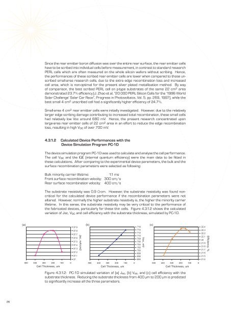
The device simulation program PC-1D was used to calculate and analyse the cell performance.<br />
The cell Voc and the IQE (internal quantum effi ciency) were the main data to be fi tted in<br />
these calculations. After comparing to the experimental device parameters, the bulk and the<br />
surface recombination parameters were selected as following:<br />
Bulk minority carrier lifetime:<br />
1.1 ms<br />
Front surface recombination velocity: 300 cm/s<br />
Rear surface recombination velocity: 400 cm/s<br />
The substrate resistivity was 0.9 Ω-cm. However, the substrate resistivity was found noncritical<br />
for the calculated device performance if the recombination parameters were not<br />
altered. However, normally the higher substrate resistivity is, the higher the minority carrier<br />
lifetime. In this sense, the substrate resistivity may be very critical to the performance <strong>of</strong><br />
the fabricated devices, particularly for these thin cells. Figure 4.3.1.2 shows the calculated<br />
variation <strong>of</strong> Jsc, Voc and cell effi ciency with the substrate thickness, simulated by PC-1D.<br />
(a) (b) (c)<br />
37.9<br />
716<br />
37.8<br />
714<br />
712<br />
37.7<br />
710<br />
37.6<br />
708<br />
37.5<br />
706<br />
37.4<br />
704<br />
37.3<br />
702<br />
700<br />
37.2<br />
698<br />
37.1<br />
696<br />
37<br />
694<br />
500<br />
400 300 200 100<br />
Cell Thickness, um<br />
0<br />
Jsc, mA/cm2<br />
500<br />
400 300 200 100<br />
Cell Thickness, um<br />
Figure 4.3.1.2: PC-1D simulated variation <strong>of</strong> (a) J sc , (b) Voc, and (c) cell effi ciency with the<br />
substrate thickness. Reducing the substrate thickness from 400 µm to 200 µm is predicted<br />
to signifi cantly increase all the three parameters.<br />
0<br />
Voc, mV<br />
500<br />
400 300 200 100<br />
Cell Thickness, um<br />
0<br />
22.4<br />
22.3<br />
22.2<br />
22.1<br />
22<br />
21.9<br />
21.8<br />
21.7<br />
21.6<br />
21.5<br />
21.4<br />
Efficiency, %<br />
26


