

Complete Report - University of New South Wales
Complete Report - University of New South Wales
Complete Report - University of New South Wales

Create successful ePaper yourself
Turn your PDF publications into a flip-book with our unique Google optimized e-Paper software.
The phonon dispersions show that if the superlattice structure is engineered correctly, the<br />
mini-gaps can in principle be arranged such that they prevent the decay <strong>of</strong> optical phonons by<br />
interrupting the same mechanism. However the density <strong>of</strong> states (DOS) in Figure 4.5.25 and<br />
Figure 4.5.26 indicate that complete gaps in the DOS for all directions in reciprocal space<br />
only occur for the QD superlattice. Hence this mechanism <strong>of</strong> slowing carrier cooling should<br />
only be present in QD structures. Experimental evidence for this in the literature is being<br />
assessed and effects on effi ciencies calculated. However, to achieve such effects in practice,<br />
the structure would need to be fi nely tuned.<br />
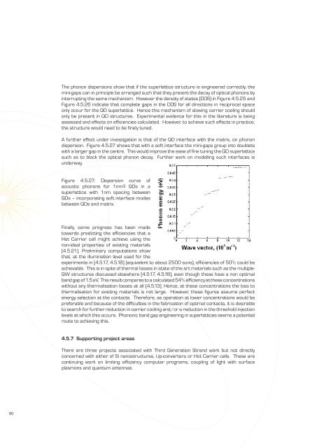
A further effect under investigation is that <strong>of</strong> the QD interface with the matrix, on phonon<br />
dispersion. Figure 4.5.27 shows that with a s<strong>of</strong>t interface the mini-gaps group into doublets<br />
with a larger gap in the centre. This would improve the ease <strong>of</strong> fi ne tuning the QD superlattice<br />
such as to block the optical phonon decay. Further work on modelling such interfaces is<br />
underway.<br />
Figure 4.5.27: Dispersion curve <strong>of</strong><br />
acoustic phonons for 1nm3 QDs in a<br />
superlattice with 1nm spacing between<br />
QDs – incorporating s<strong>of</strong>t interface modes<br />
between QDs and matrix.<br />
Finally, some progress has been made<br />
towards predicting the effi ciencies that a<br />
Hot Carrier cell might achieve using the<br />
non-ideal properties <strong>of</strong> existing materials<br />
[4.5.21]. Preliminary computations show<br />
that, at the illumination level used for the<br />
experiments in [4.5.17, 4.5.18] (equivalent to about 2500 suns), effi ciencies <strong>of</strong> 50% could be<br />
achievable. This is in spite <strong>of</strong> thermal losses in state <strong>of</strong> the art materials such as the multiple-<br />
QW structures discussed elsewhere [4.5.17, 4.5.18], even though these have a non optimal<br />
band gap <strong>of</strong> 1.5 eV. This result compares to a calculated 54% effi ciency at these concentrations<br />
without any thermalisation losses at all [4.5.13]. Hence, at these concentrations the loss to<br />
thermalisation for existing materials is not large. However, these fi gures assume perfect<br />
energy selection at the contacts. Therefore, as operation at lower concentrations would be<br />
preferable and because <strong>of</strong> the diffi culties in the fabrication <strong>of</strong> optimal contacts, it is desirable<br />
to search for further reduction in carrier cooling and/or a reduction in the threshold injection<br />
levels at which this occurs. Phononic band gap engineering in superlattices seems a potential<br />
route to achieving this.<br />
4.5.7 Supporting project areas<br />
There are three projects associated with Third Generation Strand work but not directly<br />
concerned with either <strong>of</strong> Si nanostructures, Up-converters or Hot Carrier cells. These are<br />
continuing work on limiting effi ciency computer programs, coupling <strong>of</strong> light with surface<br />
plasmons and quantum antennae.<br />
90


