

Complete Report - University of New South Wales
Complete Report - University of New South Wales
Complete Report - University of New South Wales

Create successful ePaper yourself
Turn your PDF publications into a flip-book with our unique Google optimized e-Paper software.
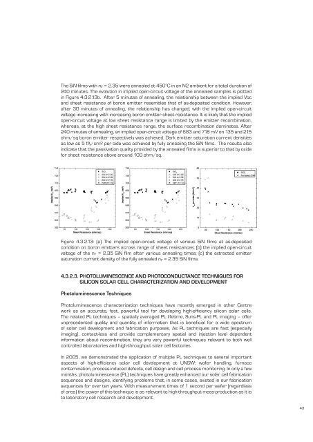
The SiN fi lms with nr = 2.35 were annealed at 450°C in an N2 ambient for a total duration <strong>of</strong><br />
240 minutes. The evolution in implied open-circuit voltage <strong>of</strong> the annealed samples is plotted<br />
in Figure 4.3.2.13b. After 5 minutes <strong>of</strong> annealing, the relationship between the implied Voc<br />
and sheet resistance <strong>of</strong> boron emitter resembles that <strong>of</strong> as-deposited condition. However,<br />
after 30 minutes <strong>of</strong> annealing, the relationship has changed, with the implied open-circuit<br />
voltage increasing with increasing boron emitter sheet resistance. It is likely that the implied<br />
open-circuit voltage at low sheet resistance range is limited by the emitter recombination,<br />
whereas, at the high sheet resistance range, the surface recombination dominates. After<br />
240 minutes <strong>of</strong> annealing, an implied open-circuit voltage <strong>of</strong> 683 and 718 mV on 135 and 215<br />
ohm/sq boron emitter respectively was achieved. Dark emitter saturation current densities<br />
as low as 5 fA/cm2 per side was achieved by fully annealing the SiN fi lms. The results also<br />
indicate that the passivation quality provided by the annealed fi lms is superior to that by oxide<br />
for sheet resistance above around 100 ohm/sq.<br />
Figure 4.3.2.13: (a) The implied open-circuit voltage <strong>of</strong> various SiN fi lms at as-deposited<br />
condition on boron emitters across range <strong>of</strong> sheet resistances; (b) the implied open-circuit<br />
voltage <strong>of</strong> the nr = 2.35 SiN fi lm after various annealing times; (c) the extracted emitter<br />
saturation current density <strong>of</strong> the fully annealed nr = 2.35 SiN fi lms.<br />
4.3.2.3. PHOTOLUMINESCENCE AND PHOTOCONDUCTANCE TECHNIQUES FOR<br />
SILICON SOLAR CELL CHARACTERIZATION AND DEVELOPMENT<br />
Photoluminescence Techniques<br />
Photoluminescence characterization techniques have recently emerged in other Centre<br />
work as an accurate, fast, powerful tool for developing high-effi ciency silicon solar cells.<br />
The related PL techniques – spatially averaged PL lifetime, Suns-PL and PL imaging – <strong>of</strong>fer<br />
unprecedented quality and quantity <strong>of</strong> information that is benefi cial for a wide spectrum<br />
<strong>of</strong> solar cell development and fabrication purposes. As PL techniques are fast (especially<br />
imaging), contact-less and provide complementary spatial and injection level dependent<br />
information about recombination, they are very powerful techniques relevant to both well<br />
controlled laboratories and high-throughput solar cell factories.<br />
In 2005, we demonstrated the application <strong>of</strong> multiple PL techniques to several important<br />
aspects <strong>of</strong> high-effi ciency solar cell development at UNSW: wafer handling, furnace<br />
contamination, process-induced defects, cell design and cell process monitoring. In only a few<br />
months, photoluminescence (PL) techniques have greatly enhanced our solar cell fabrication<br />
sequences and designs, identifying problems that, in some cases, existed in our fabrication<br />
sequences for over ten years. With measurement times <strong>of</strong> 1 second per wafer (regardless<br />
<strong>of</strong> area) the power <strong>of</strong> this technique is as relevant to high-throughput mass-production as it is<br />
to laboratory cell research and development.<br />
43


