

Complete Report - University of New South Wales
Complete Report - University of New South Wales
Complete Report - University of New South Wales

Create successful ePaper yourself
Turn your PDF publications into a flip-book with our unique Google optimized e-Paper software.
PhD student Daniel Inns inspecting EVA poly-<br />
Si thin-fi lm solar cell material fabricated on a<br />
planar sheet <strong>of</strong> glass.<br />
Silicon Quantum Dots in Silicon Nitride<br />
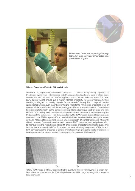
The same technique previously used to make silicon quantum dots (QDs) by deposition <strong>of</strong><br />
thin Si rich layers (4nm) interspersed with thin silicon dielectric layers, used in silicon oxide<br />
based materials, has been successfully applied to silicon nitride based materials. The lower<br />
Si 3 N 4 barrier height should give a higher interdot probability for carrier transport, thus<br />
resulting in a higher conductivity material for the same QD density. The concept will next be<br />
applied to SiC with an even lower barrier height. Transfer to nitride is an important pro<strong>of</strong> <strong>of</strong><br />
concept <strong>of</strong> the transferability <strong>of</strong> the technology to different material systems. Growth has<br />
been accomplished both by the same reactive sputtering technique used for oxide and with<br />
PECVD. On annealing, both these structures produce nanocrystals <strong>of</strong> Si limited in size by the<br />
thickness <strong>of</strong> the Si rich layer – as demonstrated by the TEM images shown. Electron density<br />
contrast for the TEM images <strong>of</strong> QDs in the nitride is lower than in oxide but the crystal planes<br />
in the Si nanocrystals can still be seen. Characterisation <strong>of</strong> nanostructures is inherently<br />
diffi cult because <strong>of</strong> the small sizes involved. Hence in 2005 there has been a signifi cant effort<br />
to improve both the resolution and breadth <strong>of</strong> nanoscale characterisation techniques. This<br />
has resulted in successful XRD <strong>of</strong> Si nanostructures which nicely complements TEM data. It<br />
both corroborates the presence <strong>of</strong> Si nanocrystals and highlights some subtle differences in<br />
lattice parameter which are useful in identifying artifacts in both TEM and XRD.<br />
(a)<br />
120kV TEM image <strong>of</strong> PECVD deposited (a) Si quantum dots in 10 bi-layers <strong>of</strong> a silicon-rich-<br />
SiNx /SiNx superlattice and (b) 300kV High Resolution TEM image showing lattice planes in<br />
Si nanocrystals.<br />
(b)<br />
5


