

Complete Report - University of New South Wales
Complete Report - University of New South Wales
Complete Report - University of New South Wales

You also want an ePaper? Increase the reach of your titles
YUMPU automatically turns print PDFs into web optimized ePapers that Google loves.
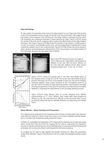
Solar Cell Design<br />
PL was used to characterize a new method <strong>of</strong> edge isolation for our n-type cells that involves<br />
a laser formed isolation trench through the emitter and around the solar cell’s edge. Several<br />
test wafers were prepared, half including the new edge isolation technique and the other<br />
half employing the traditional technique <strong>of</strong> laser-cleaving the edge. Figure 4.3.2.16 shows<br />
the results <strong>of</strong> Suns-PL and PL imaging used to analyze the effectiveness <strong>of</strong> the edge isolation<br />
technique. The image in Figure 4.3.2.16a shows the sample in high injection, revealing where,<br />
in order to create a recombination active area, we have deliberately scratched the surface<br />
outside the isolation trench with a diamond pen. Figure 4.3.2.16b shows the same sample in<br />
lower injection, demonstrating the effectiveness <strong>of</strong> the new process in providing isolation <strong>of</strong><br />
the main solar cell area from the edges and scratches.<br />
Figure 4.3.2.16: Photoluminescence images <strong>of</strong><br />
1 Ωcm, 240µm thick, n-type wafers with phosphorus<br />
diffusion on the rear side and boron diffusion on<br />
the front side with isolation trench after various<br />
processing steps: a) at ~ 1 Sun ; b) ~ 0.1 Suns<br />
Figure 4.3.2.17 shows the pseudo dark IV and dark local ideality factor <strong>of</strong><br />
the samples shown in Figure 4.3.2.16. The curves were generated using the<br />
Suns-PL technique. All <strong>of</strong> the curves labeled a) have the new trench isolation<br />
technique applied. These curves compare to the non-isolated cases b), c)<br />
and d) in which the effect <strong>of</strong> edge enhanced junction recombination and edge<br />
shunting are apparent. In this case, PL techniques provided almost immediate<br />
feedback in assessing the effectiveness <strong>of</strong> the new edge isolation process.<br />
Figure 4.3.2.17: (top) Pseudo dark I-V curves obtained from QSS-PL<br />
measurements on a 1 Ωcm, 240µm thick, n-type wafer with phosphorus<br />
diffusion on the rear side and boron diffusion on the front side after various<br />
processing steps (see text for details); (bottom) corresponding local ideality<br />
factor.<br />
Silicon Nitride – Wafer Handling and Preparation<br />
PL imaging is particularly powerful for developing silicon nitride as a passivation layer because,<br />
unlike thermal oxide fi lms, silicon nitride fi lms show a rich variety <strong>of</strong> spatially resolved effects,<br />
even in samples with exceptional quality passivation layers.<br />
In 2005, we investigated the application <strong>of</strong> PL imaging to the development <strong>of</strong> improved quality<br />
silicon nitride fi lms. We found that PL imaging can be used to understand the deposition<br />
process, to identify and address key manual handling issues, to characterize thermal annealing<br />
processes, and to study the effect <strong>of</strong> post-deposition chemical processing.<br />
PL imaging can be used to help identify how sample handling can affect the passivation<br />
quality <strong>of</strong> the SiN fi lms. Figure 4.3.2.18 shows a few PL images that highlight handling related<br />
issues.<br />
45


