

Complete Report - University of New South Wales
Complete Report - University of New South Wales
Complete Report - University of New South Wales

You also want an ePaper? Increase the reach of your titles
YUMPU automatically turns print PDFs into web optimized ePapers that Google loves.
The fact that the SPE diodes are n=1 limited strongly suggests that the voltage problem is<br />
not associated with grain boundaries or the p-n junction depletion region. Investigation <strong>of</strong><br />
the active doping levels in the base and emitter regions <strong>of</strong> the SPE cells is in progress, but it<br />
should be noted that the 393-mV SPE diode had no intentionally different doping level from<br />
that <strong>of</strong> the 463-mV SPC diode.<br />
From the results obtained in this study it is clear that SPE poly-Si material grown on AICseeded<br />
glass has a signifi cantly better crystal quality compared to SPC poly-Si material grown<br />
on bare (i.e., non-seeded) glass. So far, this advantage has not been translated into superior<br />
photovoltaic performance. Analysis <strong>of</strong> Suns-Voc curves indicates that the problem lies in the<br />
absorber region and/or the emitter region <strong>of</strong> the SPE diodes.<br />
10..0<br />
2-diode model<br />
Light Intensity (suns)<br />
1.0<br />
0.1<br />
n=1<br />
Exp. data<br />
n=2<br />
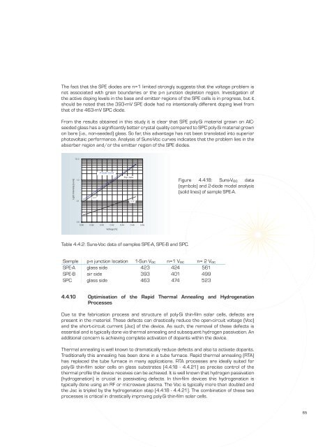
Figure 4.4.18: Suns-Voc data<br />
(symbols) and 2-diode model analysis<br />
(solid lines) <strong>of</strong> sample SPE-A.<br />
0.0<br />
0.36<br />
0.38 0.40 0.42 0.44 0.46 0.46<br />
Voltage (V)<br />
Table 4.4.2: Suns-Voc data <strong>of</strong> samples SPE-A, SPE-B and SPC.<br />
Sample p-n junction location 1-Sun Voc n=1 Voc n= 2 Voc<br />
SPE-A glass side 423 424 561<br />
SPE-B air side 393 401 499<br />
SPC glass side 463 474 523<br />
4.4.10 Optimisation <strong>of</strong> the Rapid Thermal Annealing and Hydrogenation<br />
Processes<br />
Due to the fabrication process and structure <strong>of</strong> poly-Si thin-fi lm solar cells, defects are<br />
present in the material. These defects can drastically reduce the open-circuit voltage (Voc)<br />
and the short-circuit current (Jsc) <strong>of</strong> the device. As such, the removal <strong>of</strong> these defects is<br />
essential and is typically done via thermal annealing and subsequent hydrogen passivation. An<br />
additional concern is achieving complete activation <strong>of</strong> dopants within the device.<br />
Thermal annealing is well known to dramatically reduce defects and also to activate dopants.<br />
Traditionally this annealing has been done in a tube furnace. Rapid thermal annealing (RTA)<br />
has replaced the tube furnace in many applications. RTA processes are ideally suited for<br />
poly-Si thin-fi lm solar cells on glass substrates [4.4.18 - 4.4.21] as precise control <strong>of</strong> the<br />
thermal pr<strong>of</strong>i le the device receives can be achieved. It is well known that hydrogen passivation<br />
(hydrogenation) is crucial in passivating defects. In thin-fi lm devices this hydrogenation is<br />
typically done using an RF or microwave plasma. The Voc is typically more than doubled and<br />
the Jsc is tripled by the hydrogenation step [4.4.18 - 4.4.21]. The combination <strong>of</strong> these two<br />
processes is critical in drastically improving poly-Si thin-fi lm solar cells.<br />
65


