Low_resolution_Thesis_CDD_221009_public - Visual Optics and ...
Low_resolution_Thesis_CDD_221009_public - Visual Optics and ...
Low_resolution_Thesis_CDD_221009_public - Visual Optics and ...

Create successful ePaper yourself
Turn your PDF publications into a flip-book with our unique Google optimized e-Paper software.
METHODS<br />
In both profilometers, custom algorithms were developed to extract the information<br />
(shown in a monitor <strong>and</strong> printed in paper) to a digital format, to be processed with our<br />
custom analysis algorithms (Section 2.2).<br />
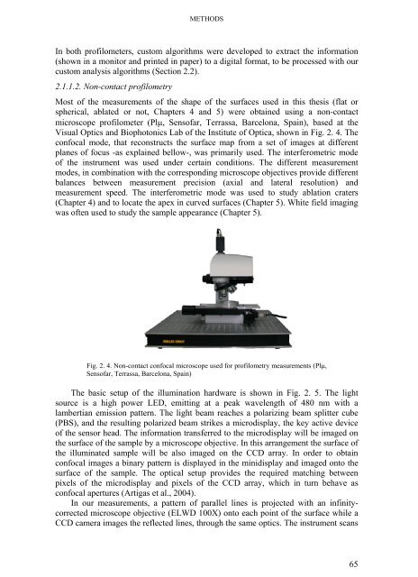
2.1.1.2. Non-contact profilometry<br />
Most of the measurements of the shape of the surfaces used in this thesis (flat or<br />
spherical, ablated or not, Chapters 4 <strong>and</strong> 5) were obtained using a non-contact<br />
microscope profilometer (Pl, Sensofar, Terrassa, Barcelona, Spain), based at the<br />
<strong>Visual</strong> <strong>Optics</strong> <strong>and</strong> Biophotonics Lab of the Institute of Optica, shown in Fig. 2. 4. The<br />
confocal mode, that reconstructs the surface map from a set of images at different<br />
planes of focus -as explained bellow-, was primarily used. The interferometric mode<br />
of the instrument was used under certain conditions. The different measurement<br />
modes, in combination with the corresponding microscope objectives provide different<br />
balances between measurement precision (axial <strong>and</strong> lateral <strong>resolution</strong>) <strong>and</strong><br />
measurement speed. The interferometric mode was used to study ablation craters<br />
(Chapter 4) <strong>and</strong> to locate the apex in curved surfaces (Chapter 5). White field imaging<br />
was often used to study the sample appearance (Chapter 5).<br />
Fig. 2. 4. Non-contact confocal microscope used for profilometry measurements (Pl,<br />
Sensofar, Terrassa, Barcelona, Spain)<br />
The basic setup of the illumination hardware is shown in Fig. 2. 5. The light<br />
source is a high power LED, emitting at a peak wavelength of 480 nm with a<br />
lambertian emission pattern. The light beam reaches a polarizing beam splitter cube<br />
(PBS), <strong>and</strong> the resulting polarized beam strikes a microdisplay, the key active device<br />
of the sensor head. The information transferred to the microdisplay will be imaged on<br />
the surface of the sample by a microscope objective. In this arrangement the surface of<br />
the illuminated sample will be also imaged on the CCD array. In order to obtain<br />
confocal images a binary pattern is displayed in the minidisplay <strong>and</strong> imaged onto the<br />
surface of the sample. The optical setup provides the required matching between<br />
pixels of the microdisplay <strong>and</strong> pixels of the CCD array, which in turn behave as<br />
confocal apertures (Artigas et al., 2004).<br />
In our measurements, a pattern of parallel lines is projected with an infinitycorrected<br />
microscope objective (ELWD 100X) onto each point of the surface while a<br />
CCD camera images the reflected lines, through the same optics. The instrument scans<br />
65