Apalis Carrier Board Design Guide - Toradex
Apalis Carrier Board Design Guide - Toradex
Apalis Carrier Board Design Guide - Toradex
- No tags were found...

Create successful ePaper yourself
Turn your PDF publications into a flip-book with our unique Google optimized e-Paper software.
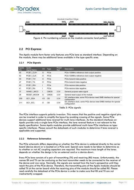
<strong>Apalis</strong> <strong>Carrier</strong> <strong>Board</strong> <strong>Design</strong> <strong>Guide</strong>Pin321Module Insertion EdgePin173Pin165Pin23Pin17 Pin1Pin320Pin174 Pin164Figure 4: Pin numbering schema on the module connector land patternPin24Pin18 Pin22.2 PCI ExpressThe <strong>Apalis</strong> module form factor only features one PCIe lane as standard interface. Depending onthe module, there may be additional lanes available in the type-specific area.2.2.1 PCIe Signals<strong>Apalis</strong>Pin<strong>Apalis</strong>Signal NameI/OTypePowerRailDescription55 PCIE1_CLK+ O PCIe PCIe 100MHz reference clock output positive53 PCIE1_CLK- O PCIe PCIe 100MHz reference clock output negative49 PCIE1_TX+ O PCIe PCIe transmit data positive47 PCIE1_TX- O PCIe PCIe transmit data negative43 PCIE1_RX+ I PCIe PCIe receive data positive41 PCIE1_RX- I PCIe PCIe receive data negative37 WAKE1_MICO I CMOS 3.3V General purpose wake signal26 RESET_MOCI# O CMOS 3.3V General reset output of the module209 I2C1_SDA I/O OD 3.3V211 I2C1_SCL O OD 3.3VI2C interface data, some PICe device need SMB interface for specialconfigurationI2C interface clock, some PICe device need SMB interface for specialconfigurationTable 3: PCIe signalsThe PCIe interface supports polarity inversion. This means that the positive and negative signal pinscan be inverted in order to simplify the layout by avoiding crossing of the signals. Some PCIedevices support additional lane reversal for multi-lane interfaces. As the standard interfaces on<strong>Apalis</strong> provide only a single lane PCIe interface, the lane reversal feature is not relevant to the<strong>Apalis</strong> specification. Some <strong>Apalis</strong> modules provide additional multi-lane PCIe interfaces as typespecificinterfaces. Please consult the datasheets of such modules to determine if lane reversal isapplicable and supported.2.2.2 Reference SchematicsThe PCIe schematic differs depending on whether the PCIe device is soldered directly to the carrierboard (device-down) or is located on a PCIe card. Special care needs to be taken to determine asto whether or not AC coupling capacitors are required. The maximum trace length of the lanesdepends on whether the design is for an external card or a device-down.Every PCIe lane consists of a pair of transmitting (TX) and receiving (RX) traces. Unfortunately, thenames RX and TX can be confusing as the host transmitter needs to be connected to the receiver ofthe device and vice versa. Normally, the signals are named from the host’s perspective until theyreach the pins of the PCIe device. Therefore, the transmitting pins of the <strong>Apalis</strong> modules should becalled TX at the carrier board while the receiving pins of the module should be called RX. Pleaseread carefully the datasheet of the PCIe device in order to make sure that RX and TX are notinadvertently swapped.<strong>Toradex</strong> AG l Altsagenstrasse 5 l 6048 Horw l Switzerland l +41 41 500 48 00 l www.toradex.com l info@toradex.com Page | 13