Apalis Carrier Board Design Guide - Toradex
Apalis Carrier Board Design Guide - Toradex
Apalis Carrier Board Design Guide - Toradex
- No tags were found...

You also want an ePaper? Increase the reach of your titles
YUMPU automatically turns print PDFs into web optimized ePapers that Google loves.
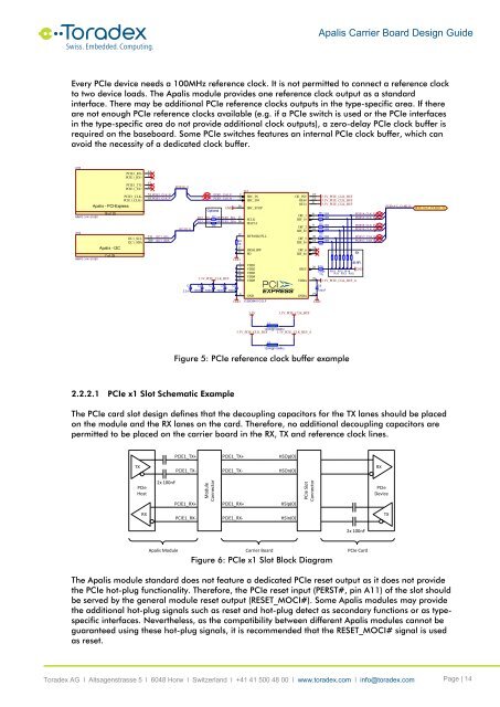
<strong>Apalis</strong> <strong>Carrier</strong> <strong>Board</strong> <strong>Design</strong> <strong>Guide</strong>Every PCIe device needs a 100MHz reference clock. It is not permitted to connect a reference clockto two device loads. The <strong>Apalis</strong> module provides one reference clock output as a standardinterface. There may be additional PCIe reference clocks outputs in the type-specific area. If thereare not enough PCIe reference clocks available (e.g. if a PCIe switch is used or the PCIe interfacesin the type-specific area do not provide additional clock outputs), a zero-delay PCIe clock buffer isrequired on the baseboard. Some PCIe switches features an internal PCIe clock buffer, which canavoid the necessity of a dedicated clock buffer.X1RPCIE1_RX-PCIE1_RX+PCIE1_TX-PCIE1_TX+PCIE1_CLK-PCIE1_CLK+<strong>Apalis</strong> - PCI-Express18 of 25MM70-314-310B1X1GI2C1_SCLI2C1_SDA<strong>Apalis</strong> - I2C7 of 25MM70-314-310B14143474953 PCIE1_CLK_N55 PCIE1_CLK_P211 I2C1_SCL209 I2C1_SDAPCIE1[0..1]IC1PCIE1_CLK_P 2SRC_INPCIE1_CLK_N 3SRC_IN#16GND SRC_STOPOptionalI2C1_SCL R2 0R PCIE1_SCL 13SCLKI2C1_SDA 0R PCIE1_SDA 14SDATAR4I2C1[0..1]12BYPASS#/PLLR91K17HIGH_BW13PDGND1VDD15VDD211VDD318VDD43.3V_PCIE_CLK_BUF 24VDD5C1 C2 C3 C4 C52.2uF 100nF 100nF 100nF 100nF4GNDGND ICS9DB401CGLFOE_INVOE6#OE1#DIF_1DIF_1#DIF_2DIF_2#DIF_5DIF_5#DIF_6DIF_6#IREFVDDAGNDA252186791020192322R1 33R33RR3R5 33R33RR6R7 33RR826 R1628475R1%C6100nF27GND3.3V_PCIE_CLK_BUF3.3V_PCIE_CLK_BUF3.3V_PCIE_CLK_BUF33RR10R11R12R13R14R153.3V_PCIE_CLK_BUF_APCIE1A_CLK_PPCIE1A_CLK_NPCIE1B_CLK_PPCIE1B_CLK_NPCIE1C_CLK_PPCIE1C_CLK_N6X49.9RGNDPCIE1A-C_CLK[0..5]PCIE1A-C_CLK[0..5]3.3V3.3V_PCIE_CLK_BUFL13A120R@100MHz3.3V_PCIE_CLK_BUF 3.3V_PCIE_CLK_BUF_AL23A120R@100MHzFigure 5: PCIe reference clock buffer example2.2.2.1 PCIe x1 Slot Schematic ExampleThe PCIe card slot design defines that the decoupling capacitors for the TX lanes should be placedon the module and the RX lanes on the card. Therefore, no additional decoupling capacitors arepermitted to be placed on the carrier board in the RX, TX and reference clock lines.PCIE1_TX+PCIE1_TX+HSOp(0)TXPCIE1_TX-PCIE1_TX-HSOn(0)RXPCIeHost2x 100nFPCIE1_RX+ModuleConnectorPCIE1_RX+HSIp(0)PCIe SlotConnectorPCIeDeviceRXPCIE1_RX-PCIE1_RX-HSIn(0)TX2x 100nF<strong>Apalis</strong> Module <strong>Carrier</strong> <strong>Board</strong> PCIe CardFigure 6: PCIe x1 Slot Block DiagramThe <strong>Apalis</strong> module standard does not feature a dedicated PCIe reset output as it does not providethe PCIe hot-plug functionality. Therefore, the PCIe reset input (PERST#, pin A11) of the slot shouldbe served by the general module reset output (RESET_MOCI#). Some <strong>Apalis</strong> modules may providethe additional hot-plug signals such as reset and hot-plug detect as secondary functions or as typespecificinterfaces. Nevertheless, as the compatibility between different <strong>Apalis</strong> modules cannot beguaranteed using these hot-plug signals, it is recommended that the RESET_MOCI# signal is usedas reset.<strong>Toradex</strong> AG l Altsagenstrasse 5 l 6048 Horw l Switzerland l +41 41 500 48 00 l www.toradex.com l info@toradex.com Page | 14