Lecture Notes for Analog Electronics - The Electronic Universe ...
Lecture Notes for Analog Electronics - The Electronic Universe ...
Lecture Notes for Analog Electronics - The Electronic Universe ...

You also want an ePaper? Increase the reach of your titles
YUMPU automatically turns print PDFs into web optimized ePapers that Google loves.
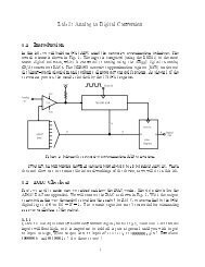
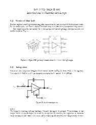
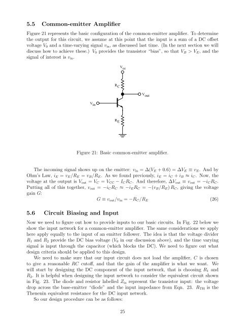
5.5 Common-emitter Amplifier<br />
Figure 21 represents the basic configuration of the common-emitter amplifier. To determine<br />
the output <strong>for</strong> this circuit, we assume at this point that the input is a sum of a DC offset<br />
voltage V0 and a time-varying signal vin, as discussed last time. (In the next section we will<br />
discuss how to achieve these.) V0 provides the transistor “bias”, so that VB >VE,andthe<br />
signal of interest is vin.<br />
V in<br />
R C<br />
R E<br />
V cc<br />
V out<br />
Figure 21: Basic common-emitter amplifier.<br />
<strong>The</strong> incoming signal shows up on the emitter: vin =∆(VE+0.6)=∆VE≡vE.Andby Ohm’s Law, iE = vE/RE = vB/RE. As we found previously, iE = iC + iB ≈ iC. Now, the<br />
voltage at the output is Vout = VC = VCC − ICRC. And there<strong>for</strong>e, ∆Vout ≡ vout = −iCRC.<br />
Putting all of this together, vout = −iCRC ≈−iERC =−(vB/RE) RC, giving the voltage<br />
gain G:<br />
G ≡ vout/vin = −RC/RE<br />
(26)<br />
5.6 Circuit Biasing and Input<br />
Now we need to figure out how to provide inputs to our basic circuits. In Fig. 22 below we<br />
show the input network <strong>for</strong> a common-emitter amplifier. <strong>The</strong> same considerations we apply<br />
here apply equally to the input of an emitter follower. <strong>The</strong> idea is that the voltage divider<br />
R1 and R2 provide the DC bias voltage (V0 in our discussion above), and the time varying<br />
signal is input through the capacitor (which blocks the DC). We need to figure out what<br />
design criteria should be applied to this design.<br />
We need to make sure that our input circuit does not load the amplifier, C is chosen<br />
to give a reasonable RC cutoff, and that the gain of the amplifier is what we want. We<br />
will start by designing the DC component of the input network, that is choosing R1 and<br />
R2. It is helpful when designing the input network to consider the equivalent circuit shown<br />
in Fig. 23. <strong>The</strong> diode and resistor labelled Zin represent the transistor input: the voltage<br />
drop across the base-emitter “diode” and the input impedance from Eqn. 23. RTH is the<br />
<strong>The</strong>nenin equivalent resistance <strong>for</strong> the DC input network.<br />
So our design procedure can be as follows:<br />
25