Lecture Notes for Analog Electronics - The Electronic Universe ...
Lecture Notes for Analog Electronics - The Electronic Universe ...
Lecture Notes for Analog Electronics - The Electronic Universe ...

Create successful ePaper yourself
Turn your PDF publications into a flip-book with our unique Google optimized e-Paper software.
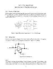
6.6.1 Gain<br />
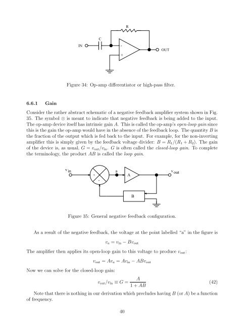
IN<br />
C<br />
-<br />
+<br />
R<br />
OUT<br />
Figure 34: Op-amp differentiator or high-pass filter.<br />
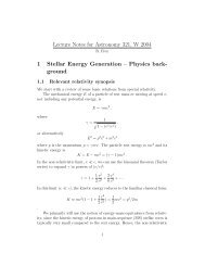
Consider the rather abstract schematic of a negative feedback amplifier system shown in Fig.<br />
35. <strong>The</strong> symbol ⊗ is meant to indicate that negative feedback is being added to the input.<br />
<strong>The</strong> op-amp device itself has intrinsic gain A. This is called the op-amp’s open-loop gain since<br />
this is the gain the op-amp would have in the absence of the feedback loop. <strong>The</strong> quantity B is<br />
the fraction of the output which is fed back to the input. For example, <strong>for</strong> the non-inverting<br />
amplifier this is simply given by the feedback voltage divider: B = R1/(R1 + R2). <strong>The</strong> gain<br />
of the device is, as usual, G = vout/vin. G is often called the closed-loop gain. Tocomplete<br />
the terminology, the product AB is called the loop gain.<br />
vin +<br />
a<br />
A<br />
vout<br />
-<br />
Figure 35: General negative feedback configuration.<br />
As a result of the negative feedback, the voltage at the point labelled “a” in the figure is<br />
B<br />
va = vin − Bvout<br />
<strong>The</strong> amplifier then applies its open-loop gain to this voltage to produce vout:<br />
Now we can solve <strong>for</strong> the closed-loop gain:<br />
vout = Ava = Avin − ABvout<br />
A<br />
vout/vin ≡ G =<br />
(42)<br />
1+AB<br />
Note that there is nothing in our derivation which precludes having B (or A) be a function<br />
of frequency.<br />
40