Lecture Notes for Analog Electronics - The Electronic Universe ...
Lecture Notes for Analog Electronics - The Electronic Universe ...
Lecture Notes for Analog Electronics - The Electronic Universe ...

Create successful ePaper yourself
Turn your PDF publications into a flip-book with our unique Google optimized e-Paper software.
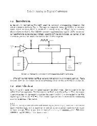
Class <strong>Notes</strong> 7<br />
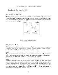
5.7 Transistor Differential Amplifier<br />
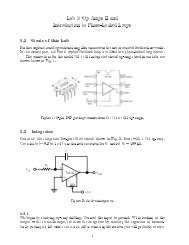
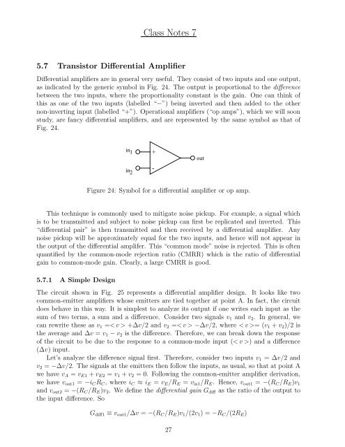
Differential amplifiers are in general very useful. <strong>The</strong>y consist of two inputs and one output,<br />
as indicated by the generic symbol in Fig. 24. <strong>The</strong> output is proportional to the difference<br />
between the two inputs, where the proportionality constant is the gain. One can think of<br />
this as one of the two inputs (labelled “−”) being inverted and then added to the other<br />
non-inverting input (labelled “+”). Operational amplifiers (“op amps”), which we will soon<br />
study, are fancy differential amplifiers, and are represented by the same symbol as that of<br />
Fig. 24.<br />
in 1<br />
in 2<br />
+<br />
-<br />
Figure 24: Symbol <strong>for</strong> a differential amplifier or op amp.<br />
This technique is commonly used to mitigate noise pickup. For example, a signal which<br />
is to be transmitted and subject to noise pickup can first be replicated and inverted. This<br />
“differential pair” is then transmitted and then received by a differential amplifier. Any<br />
noise pickup will be approximately equal <strong>for</strong> the two inputs, and hence will not appear in<br />
the output of the differential amplifer. This “common mode” noise is rejected. This is often<br />
quantified by the common-mode rejection ratio (CMRR) which is the ratio of differential<br />
gain to common-mode gain. Clearly, a large CMRR is good.<br />
5.7.1 A Simple Design<br />
<strong>The</strong> circuit shown in Fig. 25 represents a differential amplifier design. It looks like two<br />
common-emitter amplifiers whose emitters are tied together at point A. In fact, the circuit<br />
does behave in this way. It is simplest to analyze its output if one writes each input as the<br />
sum of two terms, a sum and a difference. Consider two signals v1 and v2. In general, we<br />
can rewrite these as v1 = +∆v/2 andv2 = −∆v/2, where =(v1+v2)/2is<br />
the average and ∆v = v1 − v2 is the difference. <strong>The</strong>re<strong>for</strong>e, we can break down the response<br />
of the circuit to be due to the response to a common-mode input () and a difference<br />
(∆v) input.<br />
Let’s analyze the difference signal first. <strong>The</strong>re<strong>for</strong>e, consider two inputs v1 =∆v/2 and<br />
v2=−∆v/2. <strong>The</strong> signals at the emitters then follow the inputs, as usual, so that at point A<br />
we have vA = vE1 + vE2 = v1 + v2 = 0. Following the common-emitter amplifier derivation,<br />
we have vout1 = −iCRC, whereiC ≈iE =vE/RE = vin1/RE. Hence, vout1 = −(RC/RE)v1<br />
and vout2 = −(RC/RE)v2. We define the differential gain Gdiff as the ratio of the output to<br />
the input difference. So<br />
Gdiff1 ≡ vout1/∆v = −(RC/RE)v1/(2v1) =−RC/(2RE)<br />
27<br />
out