Lecture Notes for Analog Electronics - The Electronic Universe ...
Lecture Notes for Analog Electronics - The Electronic Universe ...
Lecture Notes for Analog Electronics - The Electronic Universe ...

Create successful ePaper yourself
Turn your PDF publications into a flip-book with our unique Google optimized e-Paper software.
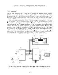
I P<br />
R P<br />
• Early Effect. VBE depends on VCE:<br />
V cc<br />
I L<br />
R L<br />
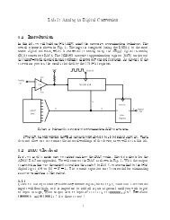
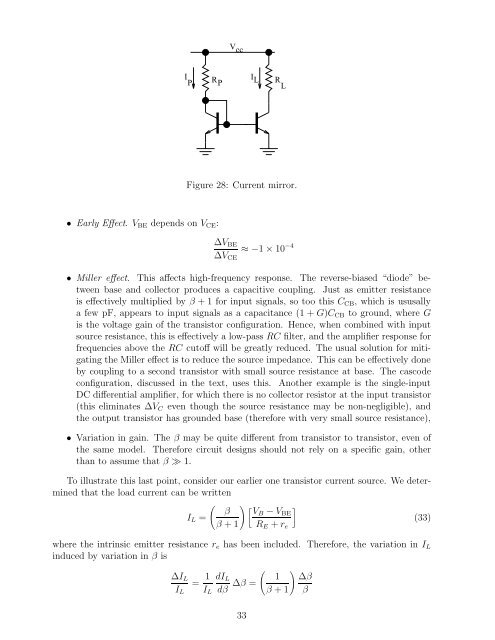
Figure 28: Current mirror.<br />
∆VBE<br />
∆VCE<br />
≈−1×10 −4<br />
• Miller effect. This affects high-frequency response. <strong>The</strong> reverse-biased “diode” between<br />
base and collector produces a capacitive coupling. Just as emitter resistance<br />
is effectively multiplied by β + 1 <strong>for</strong> input signals, so too this CCB, which is ususally<br />
a few pF, appears to input signals as a capacitance (1 + G)CCB to ground, where G<br />
is the voltage gain of the transistor configuration. Hence, when combined with input<br />
source resistance, this is effectively a low-pass RC filter, and the amplifier response <strong>for</strong><br />
frequencies above the RC cutoff will be greatly reduced. <strong>The</strong> usual solution <strong>for</strong> mitigating<br />
the Miller effect is to reduce the source impedance. This can be effectively done<br />
by coupling to a second transistor with small source resistance at base. <strong>The</strong> cascode<br />
configuration, discussed in the text, uses this. Another example is the single-input<br />
DC differential amplifier, <strong>for</strong> which there is no collector resistor at the input transistor<br />
(this eliminates ∆VC even though the source resistance may be non-negligible), and<br />
the output transistor has grounded base (there<strong>for</strong>e with very small source resistance),<br />
• Variation in gain. <strong>The</strong> β may be quite different from transistor to transistor, even of<br />
the same model. <strong>The</strong>re<strong>for</strong>e circuit designs should not rely on a specific gain, other<br />
than to assume that β ≫ 1.<br />
To illustrate this last point, consider our earlier one transistor current source. We determined<br />
that the load current can be written<br />
� ��VB �<br />
β −VBE<br />
IL =<br />
(33)<br />
β +1<br />
RE + re<br />
where the intrinsic emitter resistance re has been included. <strong>The</strong>re<strong>for</strong>e, the variation in IL<br />
induced by variation in β is<br />
∆IL<br />
IL<br />
= 1<br />
IL<br />
dIL<br />
dβ<br />
∆β =<br />
33<br />
�<br />
1<br />
�<br />
∆β<br />
β +1 β