- Page 1 and 2:
UM10139Volume 1: LPC214x User Manua
- Page 3 and 4:
UM10139Chapter 1: General informati
- Page 5 and 6:
Philips SemiconductorsVolume 1UM101
- Page 7 and 8:
Philips SemiconductorsVolume 1UM101
- Page 9 and 10:
Philips SemiconductorsVolume 1UM101
- Page 11 and 12:
Philips SemiconductorsVolume 1UM101
- Page 13 and 14:
Philips SemiconductorsVolume 1UM101
- Page 15 and 16:
Philips SemiconductorsVolume 1UM101
- Page 17 and 18:
Philips SemiconductorsVolume 1UM101
- Page 19 and 20:
Philips SemiconductorsVolume 1UM101
- Page 21 and 22:
Philips SemiconductorsVolume 1UM101
- Page 23 and 24:
Philips SemiconductorsVolume 1UM101
- Page 25 and 26:
Philips SemiconductorsVolume 1UM101
- Page 27 and 28:
Philips SemiconductorsVolume 1UM101
- Page 29 and 30:
Philips SemiconductorsVolume 1UM101
- Page 31 and 32:
Philips SemiconductorsVolume 1UM101
- Page 33 and 34:
Philips SemiconductorsVolume 1UM101
- Page 35 and 36: Philips SemiconductorsVolume 1UM101
- Page 37 and 38: Philips SemiconductorsVolume 1UM101
- Page 39 and 40: Philips SemiconductorsUM10139Volume
- Page 41 and 42: Philips SemiconductorsVolume 1UM101
- Page 43 and 44: Philips SemiconductorsVolume 1UM101
- Page 45 and 46: Philips SemiconductorsVolume 1UM101
- Page 47 and 48: Philips SemiconductorsVolume 1UM101
- Page 49 and 50: Philips SemiconductorsVolume 1UM101
- Page 51 and 52: Philips SemiconductorsVolume 1UM101
- Page 53 and 54: Philips SemiconductorsVolume 1UM101
- Page 55 and 56: Philips SemiconductorsVolume 1UM101
- Page 57 and 58: Philips SemiconductorsVolume 1UM101
- Page 59 and 60: Philips SemiconductorsVolume 1UM101
- Page 61 and 62: Philips SemiconductorsVolume 1UM101
- Page 63 and 64: Philips SemiconductorsVolume 1UM101
- Page 65 and 66: Philips SemiconductorsVolume 1UM101
- Page 67 and 68: Philips SemiconductorsVolume 1UM101
- Page 69 and 70: Philips SemiconductorsVolume 1UM101
- Page 71 and 72: Philips SemiconductorsVolume 1UM101
- Page 73 and 74: Philips SemiconductorsVolume 1UM101
- Page 75 and 76: UM10139Chapter 7: Pin Connect Block
- Page 77 and 78: Philips SemiconductorsVolume 1UM101
- Page 79 and 80: Philips SemiconductorsVolume 1UM101
- Page 81 and 82: UM10139Chapter 8: General Purpose I
- Page 83 and 84: Philips SemiconductorsVolume 1UM101
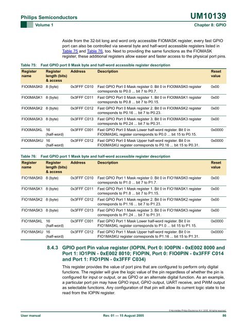
- Page 85: Philips SemiconductorsVolume 1UM101
- Page 89 and 90: Philips SemiconductorsVolume 1UM101
- Page 91 and 92: Philips SemiconductorsVolume 1UM101
- Page 93 and 94: Philips SemiconductorsVolume 1UM101
- Page 95 and 96: UM10139Chapter 9: Universal Asynchr
- Page 97 and 98: Philips SemiconductorsVolume 1UM101
- Page 99 and 100: Philips SemiconductorsVolume 1UM101
- Page 101 and 102: Philips SemiconductorsVolume 1UM101
- Page 103 and 104: Philips SemiconductorsVolume 1UM101
- Page 105 and 106: Philips SemiconductorsVolume 1UM101
- Page 107 and 108: Philips SemiconductorsVolume 1UM101
- Page 109 and 110: Philips SemiconductorsVolume 1UM101
- Page 111 and 112: Philips SemiconductorsVolume 1UM101
- Page 113 and 114: Philips SemiconductorsVolume 1UM101
- Page 115 and 116: Philips SemiconductorsVolume 1UM101
- Page 117 and 118: Philips SemiconductorsVolume 1UM101
- Page 119 and 120: Philips SemiconductorsVolume 1UM101
- Page 121 and 122: Philips SemiconductorsVolume 1UM101
- Page 123 and 124: Philips SemiconductorsVolume 1UM101
- Page 125 and 126: Philips SemiconductorsVolume 1UM101
- Page 127 and 128: Philips SemiconductorsVolume 1UM101
- Page 129 and 130: Philips SemiconductorsVolume 1UM101
- Page 131 and 132: Philips SemiconductorsVolume 1UM101
- Page 133 and 134: UM10139Chapter 11: I 2 C interfaces
- Page 135 and 136: Philips SemiconductorsVolume 1UM101
- Page 137 and 138:
Philips SemiconductorsVolume 1UM101
- Page 139 and 140:
Philips SemiconductorsVolume 1UM101
- Page 141 and 142:
Philips SemiconductorsVolume 1UM101
- Page 143 and 144:
Philips SemiconductorsVolume 1UM101
- Page 145 and 146:
Philips SemiconductorsVolume 1UM101
- Page 147 and 148:
Philips SemiconductorsVolume 1UM101
- Page 149 and 150:
Philips SemiconductorsVolume 1UM101
- Page 151 and 152:
Philips SemiconductorsVolume 1UM101
- Page 153 and 154:
Philips SemiconductorsUM10139Volume
- Page 155 and 156:
Philips SemiconductorsVolume 1UM101
- Page 157 and 158:
Philips SemiconductorsVolume 1UM101
- Page 159 and 160:
Philips SemiconductorsVolume 1UM101
- Page 161 and 162:
Philips SemiconductorsVolume 1UM101
- Page 163 and 164:
Philips SemiconductorsVolume 1UM101
- Page 165 and 166:
Philips SemiconductorsVolume 1UM101
- Page 167 and 168:
Philips SemiconductorsVolume 1UM101
- Page 169 and 170:
Philips SemiconductorsVolume 1UM101
- Page 171 and 172:
UM10139Chapter 12: SPI Interface (S
- Page 173 and 174:
Philips SemiconductorsVolume 1UM101
- Page 175 and 176:
Philips SemiconductorsVolume 1UM101
- Page 177 and 178:
Philips SemiconductorsVolume 1UM101
- Page 179 and 180:
Philips SemiconductorsVolume 1UM101
- Page 181 and 182:
Philips SemiconductorsVolume 1UM101
- Page 183 and 184:
Philips SemiconductorsVolume 1UM101
- Page 185 and 186:
Philips SemiconductorsVolume 1UM101
- Page 187 and 188:
Philips SemiconductorsVolume 1UM101
- Page 189 and 190:
Philips SemiconductorsVolume 1UM101
- Page 191 and 192:
Philips SemiconductorsVolume 1UM101
- Page 193 and 194:
Philips SemiconductorsVolume 1UM101
- Page 195 and 196:
Philips SemiconductorsVolume 1UM101
- Page 197 and 198:
Philips SemiconductorsVolume 1UM101
- Page 199 and 200:
Philips SemiconductorsVolume 1UM101
- Page 201 and 202:
Philips SemiconductorsVolume 1UM101
- Page 203 and 204:
Philips SemiconductorsVolume 1UM101
- Page 205 and 206:
Philips SemiconductorsVolume 1UM101
- Page 207 and 208:
Philips SemiconductorsVolume 1UM101
- Page 209 and 210:
Philips SemiconductorsVolume 1UM101
- Page 211 and 212:
Philips SemiconductorsVolume 1UM101
- Page 213 and 214:
Philips SemiconductorsVolume 1UM101
- Page 215 and 216:
Philips SemiconductorsVolume 1UM101
- Page 217 and 218:
Philips SemiconductorsVolume 1UM101
- Page 219 and 220:
Philips SemiconductorsVolume 1UM101
- Page 221 and 222:
Philips SemiconductorsVolume 1UM101
- Page 223 and 224:
Philips SemiconductorsVolume 1UM101
- Page 225 and 226:
Philips SemiconductorsVolume 1UM101
- Page 227 and 228:
Philips SemiconductorsVolume 1UM101
- Page 229 and 230:
Philips SemiconductorsVolume 1UM101
- Page 231 and 232:
Philips SemiconductorsVolume 1UM101
- Page 233 and 234:
Philips SemiconductorsVolume 1UM101
- Page 235 and 236:
Philips SemiconductorsVolume 1UM101
- Page 237 and 238:
Philips SemiconductorsVolume 1UM101
- Page 239 and 240:
Philips SemiconductorsVolume 1UM101
- Page 241 and 242:
Philips SemiconductorsVolume 1UM101
- Page 243 and 244:
Philips SemiconductorsVolume 1UM101
- Page 245 and 246:
Philips SemiconductorsVolume 1UM101
- Page 247 and 248:
Philips SemiconductorsVolume 1UM101
- Page 249 and 250:
Philips SemiconductorsVolume 1UM101
- Page 251 and 252:
Philips SemiconductorsVolume 1UM101
- Page 253 and 254:
UM10139Chapter 16: Pulse Width Modu
- Page 255 and 256:
Philips SemiconductorsVolume 1UM101
- Page 257 and 258:
Philips SemiconductorsVolume 1UM101
- Page 259 and 260:
Philips SemiconductorsVolume 1UM101
- Page 261 and 262:
Philips SemiconductorsVolume 1UM101
- Page 263 and 264:
Philips SemiconductorsVolume 1UM101
- Page 265 and 266:
UM10139Chapter 17: Analog-to-Digita
- Page 267 and 268:
Philips SemiconductorsVolume 1UM101
- Page 269 and 270:
Philips SemiconductorsVolume 1UM101
- Page 271 and 272:
Philips SemiconductorsVolume 1UM101
- Page 273 and 274:
UM10139Chapter 18: Digital-to-Analo
- Page 275 and 276:
UM10139Chapter 19: Real Time ClockR
- Page 277 and 278:
Philips SemiconductorsVolume 1UM101
- Page 279 and 280:
Philips SemiconductorsVolume 1UM101
- Page 281 and 282:
Philips SemiconductorsVolume 1UM101
- Page 283 and 284:
Philips SemiconductorsVolume 1UM101
- Page 285 and 286:
Philips SemiconductorsVolume 1UM101
- Page 287 and 288:
UM10139Chapter 20: Watchdog TimerRe
- Page 289 and 290:
Philips SemiconductorsVolume 1UM101
- Page 291 and 292:
UM10139Chapter 21: Flash Memory Sys
- Page 293 and 294:
Philips SemiconductorsVolume 1UM101
- Page 295 and 296:
Philips SemiconductorsVolume 1UM101
- Page 297 and 298:
Philips SemiconductorsVolume 1UM101
- Page 299 and 300:
Philips SemiconductorsVolume 1UM101
- Page 301 and 302:
Philips SemiconductorsVolume 1UM101
- Page 303 and 304:
Philips SemiconductorsVolume 1UM101
- Page 305 and 306:
Philips SemiconductorsVolume 1UM101
- Page 307 and 308:
Philips SemiconductorsVolume 1UM101
- Page 309 and 310:
Philips SemiconductorsVolume 1UM101
- Page 311 and 312:
Philips SemiconductorsVolume 1UM101
- Page 313 and 314:
Philips SemiconductorsVolume 1UM101
- Page 315 and 316:
UM10139Chapter 23: Embedded Trace M
- Page 317 and 318:
Philips SemiconductorsVolume 1UM101
- Page 319 and 320:
UM10139Chapter 24: RealMonitorRev.
- Page 321 and 322:
Philips SemiconductorsVolume 1UM101
- Page 323 and 324:
Philips SemiconductorsVolume 1UM101
- Page 325 and 326:
Philips SemiconductorsVolume 1UM101
- Page 327 and 328:
Philips SemiconductorsVolume 1UM101
- Page 329 and 330:
UM10139Chapter 25: Supplementary in
- Page 331 and 332:
Philips SemiconductorsVolume 1UM101
- Page 333 and 334:
Philips SemiconductorsVolume 1UM101
- Page 335 and 336:
Philips SemiconductorsVolume 1UM101
- Page 337 and 338:
Philips SemiconductorsVolume 1UM101
- Page 339 and 340:
Philips SemiconductorsVolume 1UM101
- Page 341 and 342:
Philips SemiconductorsVolume 1UM101
- Page 343 and 344:
Philips SemiconductorsVolume 1UM101
- Page 345 and 346:
Philips SemiconductorsVolume 1UM101
- Page 347 and 348:
Philips SemiconductorsVolume 1UM101


![[1.1] Syringe Tool Linear Motor [1.2] X Axis Linear ... - Fab@Home](https://img.yumpu.com/11541747/1/184x260/11-syringe-tool-linear-motor-12-x-axis-linear-fabhome.jpg?quality=85)