Qualification of the Assembly Process of Flip-Chip BGA Packages ...
Qualification of the Assembly Process of Flip-Chip BGA Packages ...
Qualification of the Assembly Process of Flip-Chip BGA Packages ...

Create successful ePaper yourself
Turn your PDF publications into a flip-book with our unique Google optimized e-Paper software.
Texas Tech University, Nivetha Shivan, May 2012<br />
This gives us an edge over Phase I, as we can also test <strong>the</strong> parts electrically to make sure<br />
<strong>the</strong> new package has no impact on <strong>the</strong> electrical behavior <strong>of</strong> <strong>the</strong> die inside.<br />
Phase II also introduces ano<strong>the</strong>r variable, a change in <strong>the</strong> wafer fabrication technology<br />
called Nitride Seal Mask (NSM).<br />
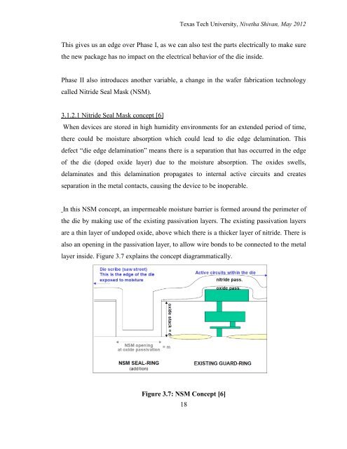
3.1.2.1 Nitride Seal Mask concept [6]<br />
When devices are stored in high humidity environments for an extended period <strong>of</strong> time,<br />
<strong>the</strong>re could be moisture absorption which could lead to die edge delamination. This<br />
defect “die edge delamination” means <strong>the</strong>re is a separation that has occurred in <strong>the</strong> edge<br />
<strong>of</strong> <strong>the</strong> die (doped oxide layer) due to <strong>the</strong> moisture absorption. The oxides swells,<br />
delaminates and this delamination propagates to internal active circuits and creates<br />
separation in <strong>the</strong> metal contacts, causing <strong>the</strong> device to be inoperable.<br />
In this NSM concept, an impermeable moisture barrier is formed around <strong>the</strong> perimeter <strong>of</strong><br />
<strong>the</strong> die by making use <strong>of</strong> <strong>the</strong> existing passivation layers. The existing passivation layers<br />
are a thin layer <strong>of</strong> undoped oxide, above which <strong>the</strong>re is a thicker layer <strong>of</strong> nitride. There is<br />
also an opening in <strong>the</strong> passivation layer, to allow wire bonds to be connected to <strong>the</strong> metal<br />
layer inside. Figure 3.7 explains <strong>the</strong> concept diagrammatically.<br />
Figure 3.7: NSM Concept [6]<br />
18