Qualification of the Assembly Process of Flip-Chip BGA Packages ...
Qualification of the Assembly Process of Flip-Chip BGA Packages ...
Qualification of the Assembly Process of Flip-Chip BGA Packages ...

Create successful ePaper yourself
Turn your PDF publications into a flip-book with our unique Google optimized e-Paper software.
Texas Tech University, Nivetha Shivan, May 2012<br />
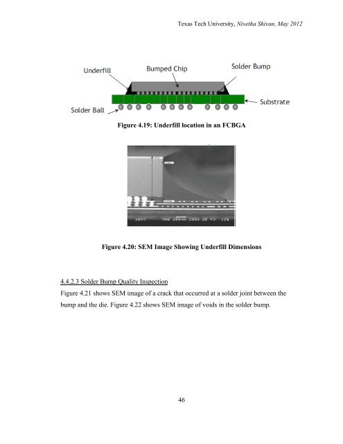
Figure 4.19: Underfill location in an FC<strong>BGA</strong><br />
Figure 4.20: SEM Image Showing Underfill Dimensions<br />
4.4.2.3 Solder Bump Quality Inspection<br />
Figure 4.21 shows SEM image <strong>of</strong> a crack that occurred at a solder joint between <strong>the</strong><br />
bump and <strong>the</strong> die. Figure 4.22 shows SEM image <strong>of</strong> voids in <strong>the</strong> solder bump.<br />
46