Qualification of the Assembly Process of Flip-Chip BGA Packages ...
Qualification of the Assembly Process of Flip-Chip BGA Packages ...
Qualification of the Assembly Process of Flip-Chip BGA Packages ...

You also want an ePaper? Increase the reach of your titles
YUMPU automatically turns print PDFs into web optimized ePapers that Google loves.
Texas Tech University, Nivetha Shivan, May 2012<br />
Figure 6.1: CSAM Image Showing White Area in Underfill Region<br />
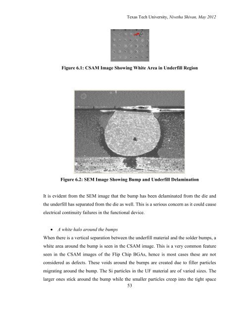
Figure 6.2: SEM Image Showing Bump and Underfill Delamination<br />
It is evident from <strong>the</strong> SEM image that <strong>the</strong> bump has been delaminated from <strong>the</strong> die and<br />
<strong>the</strong> underfill has separated from <strong>the</strong> die as well. This is a serious concern as it could cause<br />
electrical continuity failures in <strong>the</strong> functional device.<br />
� A white halo around <strong>the</strong> bumps<br />
When <strong>the</strong>re is a vertical separation between <strong>the</strong> underfill material and <strong>the</strong> solder bumps, a<br />
white area around <strong>the</strong> bump is seen in <strong>the</strong> CSAM image. This is a very common feature<br />
seen in <strong>the</strong> CSAM images <strong>of</strong> <strong>the</strong> <strong>Flip</strong> <strong>Chip</strong> <strong>BGA</strong>s, hence is most cases <strong>the</strong>se are not<br />
considered as defects. These voids around <strong>the</strong> bumps are created due to filler particles<br />
migrating around <strong>the</strong> bump. The Si particles in <strong>the</strong> UF material are <strong>of</strong> varied sizes. The<br />
larger ones stick around <strong>the</strong> bump while <strong>the</strong> smaller particles creep into <strong>the</strong> tight space<br />
53