Qualification of the Assembly Process of Flip-Chip BGA Packages ...
Qualification of the Assembly Process of Flip-Chip BGA Packages ...
Qualification of the Assembly Process of Flip-Chip BGA Packages ...

You also want an ePaper? Increase the reach of your titles
YUMPU automatically turns print PDFs into web optimized ePapers that Google loves.
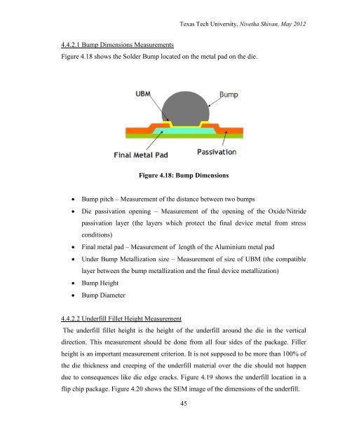
4.4.2.1 Bump Dimensions Measurements<br />
Texas Tech University, Nivetha Shivan, May 2012<br />
Figure 4.18 shows <strong>the</strong> Solder Bump located on <strong>the</strong> metal pad on <strong>the</strong> die.<br />
Figure 4.18: Bump Dimensions<br />
� Bump pitch – Measurement <strong>of</strong> <strong>the</strong> distance between two bumps<br />
� Die passivation opening – Measurement <strong>of</strong> <strong>the</strong> opening <strong>of</strong> <strong>the</strong> Oxide/Nitride<br />
passivation layer (<strong>the</strong> layers which protect <strong>the</strong> final device metal from stress<br />
conditions)<br />
� Final metal pad – Measurement <strong>of</strong> length <strong>of</strong> <strong>the</strong> Aluminium metal pad<br />
� Under Bump Metallization size – Measurement <strong>of</strong> size <strong>of</strong> UBM (<strong>the</strong> compatible<br />
layer between <strong>the</strong> bump metallization and <strong>the</strong> final device metallization)<br />
� Bump Height<br />
� Bump Diameter<br />
4.4.2.2 Underfill Fillet Height Measurement<br />
The underfill fillet height is <strong>the</strong> height <strong>of</strong> <strong>the</strong> underfill around <strong>the</strong> die in <strong>the</strong> vertical<br />
direction. This measurement should be done from all four sides <strong>of</strong> <strong>the</strong> package. Filler<br />
height is an important measurement criterion. It is not supposed to be more than 100% <strong>of</strong><br />
<strong>the</strong> die thickness and creeping <strong>of</strong> <strong>the</strong> underfill material over <strong>the</strong> die should not happen<br />
due to consequences like die edge cracks. Figure 4.19 shows <strong>the</strong> underfill location in a<br />
flip chip package. Figure 4.20 shows <strong>the</strong> SEM image <strong>of</strong> <strong>the</strong> dimensions <strong>of</strong> <strong>the</strong> underfill.<br />
45