mitac 8599.pdf - tim.id.au
mitac 8599.pdf - tim.id.au
mitac 8599.pdf - tim.id.au

Create successful ePaper yourself
Turn your PDF publications into a flip-book with our unique Google optimized e-Paper software.
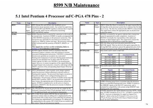
HIT#<br />
8599 N/B Maintenance<br />
5.1 Intel Pentium 4 Processor mFC-PGA 478 Pins - 2<br />
Name Type Description<br />
Input/<br />
Output<br />
HIT# (Snoop Hit) and HITM# (Hit Modified) convey<br />
transaction snoop operation results. Any system bus agent may<br />
assert both HIT# and HITM# together to indicate that it requires<br />
a snoop stall, which can be continued by reasserting<br />
HITM#<br />
IERR#<br />
Input/<br />
Output HIT# and HITM# together.<br />
Output IERR# (Internal Error) is asserted by a processor as the result of<br />
an internal error. Assertion of IERR# is usually accompanied by<br />
a SHUTDOWN transaction on the processor system bus. This<br />
transaction may optionally be converted to an external error<br />
signal (e.g., NMI) by system core logic. The processor will keep<br />
IERR# asserted until the assertion of RESET#, BINIT#, or<br />
INIT#.<br />
This signals does not have on-die termination. Refer to<br />
Section 2.5 fortermination requirements.<br />
IGNNE#<br />
Input IGNNE# (Ignore Numeric Error) is asserted to force the<br />
processor to ignore a numeric error and continue to execute<br />
noncontrol floating-point instructions. If IGNNE# is deasserted,<br />
the processor generates an exception on a noncontrol<br />
floating-point instruction if a previous floating-point instruction<br />
c<strong>au</strong>sed an error.IGNNE# has no effect when the NE bit in<br />
control register 0 (CR0) is set. IGNNE# is an asynchronous<br />
signal. However, to ensure recognition of this signal following<br />
an Input/Output write instruction, it must be val<strong>id</strong> along with the<br />
TRDY# assertion of the corresponding Input/Output Write bus<br />
transaction.<br />
INIT#<br />
Input INIT# (Initialization), when asserted, resets integer registers<br />
ins<strong>id</strong>e the processor without affecting its internal caches or<br />
floating-point registers. The processor then begins execution at<br />
the power-on Reset vector configured during power-on<br />
configuration. The processor continues to handle snoop requests<br />
during INIT# assertion. INIT# is an asynchronous signal and<br />
must connect the appropriate pins of all processor system bus<br />
agents. If INIT# is sampled active on the active to inactive<br />
transition of RESET#, then the processor executes its Built-in<br />
Self-Test (BIST).<br />
ITPCLKOUT[1:0] Output The ITPCLKOUT[1:0] pins do not prov<strong>id</strong>e any output for the<br />
Pentium® 4 processor in the 478-pin package. Refer to Section<br />
2.5 for additional details and termination requirements.<br />
ITP_CLK[1:0] Input ITP_CLK[1:0] are copies of BCLK that are used only in<br />
processor systems where no debug port is implemented on the<br />
system board. ITP_CLK[1:0] are used as BCLK[1:0] references<br />
for a debug port implemented on an interposer. If a debug port<br />
is implemented in the system, ITP_CLK[1:0] are no connects in<br />
the system. These are not processor signals.<br />
DBSY#<br />
DEFER#<br />
DP[3:0]#<br />
DSTBN[3:0]#<br />
Name Type Description<br />
Input/<br />
Output<br />
Input<br />
Input/<br />
Output<br />
Input/<br />
Output<br />
DSTBP[3:0]# Input/<br />
Output<br />
FERR#<br />
GTLREF<br />
Output<br />
DBSY# (Data Bus Busy) is asserted by the agent responsible for<br />
driving data on the processor system bus to indicate that the data<br />
bus is in use. The data bus isreleased after DBSY# is deasserted.<br />
This signal must connect the appropriate pins on all processor<br />
system bus agents.<br />
DEFER# is asserted by an agent to indicate that a transaction<br />
cannot be guaranteed in-order completion. Assertion of<br />
DEFER# is normally the responsibility of the addressed<br />
memory or Input/Output agent. This signal must connect the<br />
appropriate pins of all processor system bus agents.<br />
DP[3:0]# (Data parity) prov<strong>id</strong>e parity protection for the<br />
D[63:0]# signals. They are driven by the agent responsible for<br />
driving D[63:0]#, and must connect the appropriate pins of all<br />
Pentium 4 processor in the 478-pin package system bus gents.<br />
Data strobe used to latch in D[63:0]#.<br />
Signals Associated Strobe<br />
D[15:0]#, DBI0# DSTBN0#<br />
D[31:16]#, DBI1# DSTBN1#<br />
D[47:32]#, DBI2# DSTBN2#<br />
D[63:48]#, DBI3# DSTBN3#<br />
Data strobe used to latch in D[63:0]#.<br />
Signals Associated Strobe<br />
D[15:0]#, DBI0# DSTBP0#<br />
D[31:16]#, DBI1# DSTBP1#<br />
D[47:32]#, DBI2# DSTBP2#<br />
D[63:48]#, DBI3# DSTBP3#<br />
FERR# (Floating-point Error) is asserted when the processor<br />
detects an unmasked floating-point error. FERR# is similar to<br />
the ERROR# signal on the Intel 387 coprocessor, and is<br />
included for compatibility with systems using MSDOS*-type<br />
floating-point error reporting.<br />
Input GTLREF determines the signal reference level for AGTL+ input<br />
pins. GTLREF should be set at 2/3 VCC. GTLREF is used by the<br />
AGTL+ receivers to determine if a signal is a logical 0 or<br />
logical 1. Refer to the Intel® Pentium® 4 Processor in the<br />
478-pin Package and Intel® 850 Chipset Platform Design<br />
Gu<strong>id</strong>e for more information.<br />
74