mitac 8599.pdf - tim.id.au
mitac 8599.pdf - tim.id.au
mitac 8599.pdf - tim.id.au

You also want an ePaper? Increase the reach of your titles
YUMPU automatically turns print PDFs into web optimized ePapers that Google loves.
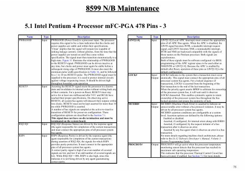
Name Type Description<br />
PWRGOOD Input PWRGOOD (Power Good) is a processor input. The processor<br />
requires this signal to be a clean indication that the clocks and<br />
power supplies are stable and within their specifications.<br />
‘Clean’ implies that the signal will remain low (capable of<br />
sinking leakage current), without glitches, from the <strong>tim</strong>e that the<br />
power supplies are turned on until they come within<br />
specification. The signal must then transition monotonically to a<br />
high state. Figure 11 illustrates the relationship of PWRGOOD<br />
to the RESET# signal. PWRGOOD can be driven inactive at<br />
any <strong>tim</strong>e, but clocks and power must again be stable before a<br />
subsequent rising edge of PWRGOOD. It must also meet the<br />
minimum pulse w<strong>id</strong>th specification in Table 16, and be followed<br />
by a 1 to 10 ms RESET# pulse. The PWRGOOD signal must be<br />
supplied to the processor; it is used to protect internal circuits<br />
against voltage sequencing issues. It should be driven high<br />
throughout boundary scan operation.<br />
RESET#<br />
Input Asserting the RESET# signal resets the processor to a known<br />
state and inval<strong>id</strong>ates its internal caches without writing back any<br />
of their contents. For a power-on Reset, RESET# must stay<br />
active for at least one millisecond after VCC and BCLK have<br />
reached their proper specifications. On observing active<br />
RESET#, all system bus agents will deassert their outputs within<br />
two clocks. RESET# must not be kept asserted for more than 10<br />
ms while PWRGOOD is asserted.<br />
A number of bus signals are sampled at the active-to-inactive<br />
transition of RESET# for power-on configuration. These<br />
configuration options are described in the Section 7.1.<br />
This signal does not have on-die termination and must be<br />
terminated on the system board.<br />
RS[2:0]#<br />
Input RS[2:0]# (Response Status) are driven by the response agent<br />
(the agent responsible for completion of the current transaction),<br />
and must connect the appropriate pins of all processor system<br />
bus agents.<br />
RSP#<br />
Input RSP# (Response Parity) is driven by the response agent (the<br />
agent responsible for completion of the current transaction)<br />
during assertion of RS[2:0]#, the signals for which RSP#<br />
prov<strong>id</strong>es parity protection. It must connect to the appropriate<br />
pins of all processor system bus agents.<br />
A correct parity signal is high if an even number of covered<br />
signals are low and low if an odd number of covered signals are<br />
low. While RS[2:0]# = 000, RSP# is also high, since this<br />
indicates it is not being driven by any agent guaranteeing<br />
correct parity.<br />
8599 N/B Maintenance<br />
5.1 Intel Pentium 4 Processor mFC-PGA 478 Pins - 3<br />
Name Type Description<br />
LINT[1:0] Input LINT[1:0] (Local APIC Interrupt) must connect the appropriate<br />
pins of all APIC Bus agents. When the APIC is disabled, the<br />
LINT0 signal becomes INTR, a maskable interrupt request<br />
signal, and LINT1 becomes NMI, a nonmaskable interrupt.<br />
INTR and NMI are backward compatible with the signals of<br />
those names on the Pentium processor. Both signals are<br />
asynchronous.<br />
Both of these signals must be software configured via BIOS<br />
programming of the APIC register space to be used either as<br />
NMI/INTR or LINT[1:0]. Bec<strong>au</strong>se the APIC is enabled by<br />
def<strong>au</strong>lt after Reset, operation of these pins as LINT[1:0] is the<br />
def<strong>au</strong>lt configuration.<br />
LOCK#<br />
Input/ LOCK# indicates to the system that a transaction must occur<br />
Output atomically. This signal must connect the appropriate pins of all<br />
processor system bus agents. For a locked sequence of<br />
transactions, LOCK# is asserted from the beginning of the<br />
first transaction to the end of the last transaction.<br />
When the priority agent asserts BPRI# to arbitrate for ownership<br />
of the processor system bus, it will wait until it observes<br />
LOCK# deasserted. This enables symmetric agents to retain<br />
ownership of the processor system bus throughout the bus<br />
locked operation and ensure the atomicity of lock.<br />
MCERR# Input/<br />
Output<br />
MCERR# (Machine Check Error) is asserted to indicate an<br />
unrecoverable error without a bus protocol violation. It may be<br />
driven by all processor system bus agents.<br />
MCERR# assertion conditions are configurable at a system<br />
level. Assertion options are defined by the following options:<br />
Enabled or disabled.<br />
Asserted, if configured, for internal errors along with IERR#.<br />
Asserted, if configured, by the request initiator of a bus<br />
transaction after it observes an error.<br />
Asserted by any bus agent when it observes an error in a bus<br />
transaction.<br />
For more details regarding machine check architecture, please<br />
refer to the IA-32 Software Developer’s Manual, Volume 3:<br />
System Programming Gu<strong>id</strong>e.<br />
PROCHOT# Output PROCHOT# will go active when the processor temperature<br />
monitoring sensor detects that the processor has reached its<br />
maximum safe operating temperature.<br />
This indicates that the processor Thermal Control Circuit has<br />
been activated, if enabled. See Section 7.3 for more details.<br />
75