mitac 8599.pdf - tim.id.au
mitac 8599.pdf - tim.id.au
mitac 8599.pdf - tim.id.au

Create successful ePaper yourself
Turn your PDF publications into a flip-book with our unique Google optimized e-Paper software.
8599 N/B Maintenance<br />
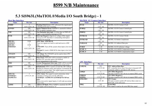
5.3 SiS963L(MuTIOL®Media I/O South Br<strong>id</strong>ge) - 1<br />
Host Bus Interface<br />
Name Pin Attr Description<br />
FERR# I<br />
0.8V/2.65V -M<br />
IGNNE# OD<br />
0.8V/2.65V -M<br />
NMI OD<br />
0.8V/2.65V -M<br />
INTR OD<br />
0.8V/2.65V -M<br />
APICD1 /<br />
GPIOFF#<br />
APICD0 /<br />
THERM2#<br />
I/OD<br />
I<br />
I/OD<br />
I<br />
0.8V/2.65V -M<br />
CPUSLP# OD<br />
0.8V/2.65V -M<br />
STPCLK# OD<br />
0.8V/2.65V -M<br />
SMI# OD<br />
0.8V/2.65V -M<br />
INIT# OD<br />
0.8V/2.65V -M<br />
APICCK/<br />
LDTREQ# /<br />
AGPBUSY#<br />
I<br />
2.5V/3.3V -M<br />
A20M# OD<br />
0.8V/2.65V- M<br />
Floating Point Error: CPU will assert this signal upon<br />
a floating point error occurring.<br />
Ignore Numeric Error: IGNNE# is asserted to inform<br />
CPU to ignore a numeric error.<br />
Non-Maskable Interrupt: A rising edge on NMI will<br />
trigger a non-maskable interrupt to CPU.<br />
Interrupt Request: High-level voltage of this signal<br />
conveys to CPU that there is outstanding interrupt(s)<br />
needed to be serviced.<br />
APIC Data: APICD[1:0]<br />
These two signals are used to send and receive APIC<br />
data.<br />
GPIO OFF: Turn off the system when input a low level<br />
signal.<br />
Thermal 2: Assert a SMI#/SCI# when input a low level<br />
signal.<br />
CPU Sleep: The CPUSLP# can be used to force CPU<br />
enter the Sleep state.<br />
Stop Clock: STPCLK# will be asserted to inhibit or<br />
throttle CPU activities upon a pre-defined<br />
power management event occurs.<br />
System Management Interrupt: SMI# will be asserted<br />
when a pre-defined power management event occurs.<br />
Initialization: INIT is used to re-start the CPU without<br />
flushing its internal caches and registers. In Pentium III<br />
platform it is active high. This signal requires an external<br />
pull-up resistor tied to VTT.<br />
APIC Clock: This signal is used to determine when<br />
val<strong>id</strong> data is being sent over the APCI bus.<br />
LDTREQ# / AGPBUSY# (LDTREQ# for K8 use<br />
only)<br />
When a low active signal inputs, it will wake up system<br />
from C3/S1.<br />
Address 20 Mask: When A20M# is asserted, the CPU<br />
A20 signal will be forced to “0”<br />
MuTIOL 1G Connect Interface<br />
Name Pin Attr Description<br />
ZCLK I<br />
3.3V - M<br />
MuTIOL 1G I/O Connect Clock<br />
ZUREQ I/O<br />
1.8V - M<br />
MuTIOL 1G I/O Conect Controll pins<br />
ZDREQ I/O<br />
1.8V - M<br />
MuTIOL 1G I/O Conect Controll pins<br />
ZSTB[1:0] I/O<br />
1.8V - M<br />
MuTIOL 1G I/O Connect Strobe<br />
ZSTB[1:0]# I/O<br />
1.8V - M<br />
MuTIOL 1G Strobe Compliment<br />
ZAD[16:0] I/O<br />
1.8V - M<br />
MuTIOL 1G Address/Data pins<br />
ZVREF I -M MuTIOL 1G I/O reference voltage<br />
ZCMP_N I -M MuTIOL 1G N-MOS Compensation Input<br />
ZCMP_P I -M MuTIOL 1G P-MOS Compensation input<br />
LPC Interface<br />
Name Pin Attr Description<br />
LAD[3:0] I/O<br />
3.3V/5V-M<br />
LDRQ# I<br />
3.3V/5V-M<br />
LDRQ1#<br />
I<br />
(GPIO1)<br />
3.3V/5V-M<br />
LFRAME# O<br />
3.3V -M<br />
SIRQ I/O<br />
3.3V/5V -M<br />
LPC Address/Data Bus:<br />
LPC controller drives these four pins to transmit LPC<br />
command, address, and data to LPC device.<br />
LPC DMA Request 0:<br />
This pin is used by LPC device to request DMA cycle.<br />
LPC DMA Request 1:<br />
This pin is used by LPC device to request DMA cycle.<br />
LPC Frame:<br />
This pin is used to notify LPC device that a start or a<br />
abort LPC cycle will occur.<br />
Serial IRQ:<br />
This signal is used as the serial IRQ line signal.<br />
83